01
-
Soldering Techniques
- 1.1 Introduction to Soldering Techniques
This guide will help students to understand and gain effective results when soldering electronic components such as light-emitting diodes (LEDs), capacitors, transistors, resistors, and etc.
Soldering is used to fix components permanently to a circuit. However, soldering requires a lot of practice if you have little or no experience of using a soldering iron. An alloy of lead and tin called solder is generally used to fix a component pin or leg to a printed circuit board (PCB).
How to make the perfect solder joint and soldering troubleshooting guide are discussed in this section. - 1.1 Introduction to Soldering Techniques
-
Soldering Techniques
- 1.2 Guidelines for a Perfect Solder Joint
a) Get ready to solder.
Make sure soldering iron is in good condition. Solder joint condition varies greatly depending on the condition of the tip of the solder iron and generally they should look clean and not burnt.
The selection of correct solder is also important. For electronic work, most importantly, you are advised to use rosin core solder to prevent traces on the printed circuit board and erode the component leads.
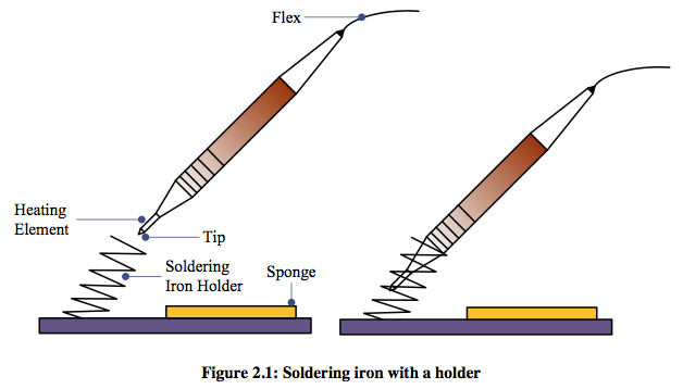
Figure 1 shows a soldering iron with a holder. It is important to tinning the soldering tip before use and these can be done by following simple steps; warm up the iron, arrange a space to work, thoroughly coat the tip in solder and clean the soldering tip.
b) Surface Preparation
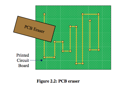
It is important to clean all surfaces to be soldered. You could use Brite pads or approved surface
cleaning material to clean the surface to remove tarnish that may have built up on the solder pad. Also, a PCB eraser could be used to clean/remove any film from the tracks as illustrated in Figure 2.
c) Component Placement
Now the board and components are cleaned and ready to place onto the solder pad. In general you will be soldering a few components at a time and start with smallest components such as diodes, resistors, LEDs, and etc. which will keep the solder pad more stable during the soldering. You could use masking tape or may want to bend the leads to hold the component in place while soldering.
d) Apply Heat and Solder to the Joint
It is recommended to apply a very small amount of solder to the tip of iron which will help to conduct the heat to the board and component. It is important to heat the lead and the board to make up the joint. The small amount of solder applied to the solder iron tip will ensure a proper contact between the lead and the pad. In general, within a second or two the joint will get hot enough to solder and do not overheat the board. When the component lead and the solder pad have heated up enough bring the tip of the solder iron to the solder pad and the component lead.
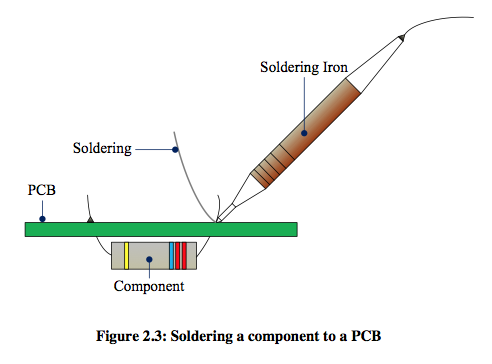
At this stage if required heat is applied the solder should flow around the lead and pad as shown in Figure 3.
e) Check the Joint and Clean-up
Once the soldering is finished check the joint for shorts with adjacent solder pads or poor flow. Extended legs on the components need to be trimmed using wire clippers and clean the excess flux residue from the board. - 1.2 Guidelines for a Perfect Solder Joint
-
Soldering – Summary
- * All the components must be clean and free from dirt.
* Keep solder pad firm, if needed use a bull clip.
* If you are using the soldering iron for the first time, apply small amount of “Tin” on the iron tip.
* Clean the tip of the solder iron using the damp sponge.
* If necessary add a small amount of fresh solder to the cleaned tip.
* Heat all parts (under a second).
* Continue heating while applying solder to form a satisfactory joint.
* Allow some time to cool the joint and inspect and clean. - * All the components must be clean and free from dirt.
-
Soldering – Troubleshooting Guide
- Common soldering problems are cold joint, insufficient wetting, too much solder, and etc.
* It is important to clean up the parts thoroughly before soldering.
* A properly pre-heated soldering iron will avoid cold joints.
* Cleaning of the joint, appropriate preparation, clean components and hot soldering iron will help prevent overheated joints.
* Even heating of both component lead and the solder pad and also cleaning will prevent insufficient wetting (pad and lead).
* If you made a mistake reheat the joint and add more solder to make a perfect joint.
* If too much solder is presented use a solder-sucker to clean.
* Trim all excess leads for a better finish.
* Use only enough solder to make a good joint to prevent unnecessary solder bridge.
CAUTION!!!
The flux in the solder will release fumes when heated which are harmful to your eyes and lungs. Hot solder is also dangerous. Therefore, always ensure good ventilation and sufficient work area to avoid breathing the smoke created. Eye protection is also advised.
Incorrect use of any machine tools may result in severe injury or death, mandatory observance to all safety rules is required. - Common soldering problems are cold joint, insufficient wetting, too much solder, and etc.
-
-
Introduction to Digital Electronics – Circuit Construction
- Aim
The purpose of the lab is to introduce the basic skills involved in handling electronic components, digital principles, the use of test equipment, interpretation of a circuit diagram and the use of prototyping methods. For further information about logic gates and the pin connections to the integrated circuits, see Appendix 5.
- Procedure
Complete the circuit diagram shown in Figure 3.1.
For all the circuits you will need the following components.
* 1 x Breadboard
* 3 x Microswitches (Note these are NORMALLY CLOSED switches)
* 1 x LED (Light emitting diode)
* 1 x AND gate 74LS08 (for pin configuration see below)
* 1 x OR gate 74LS32 (for pin configuration see below)
* 1 x Inverter 74LS05 (for pin configuration see below)
* 3 x 10kΩ resistors
* 1 x 220Ω resistor
* Solid core wire
Details of the logic tables, and pin connections associated with the AND, OR and INVERTER gates, are shown below.
- Operation
1. Construct the Right hand Side of Figure 3.1 as shown below. Do this on the right-hand side of your breadboard. That is the part to the right of the inverter with the 220Ω resistor and the LED.
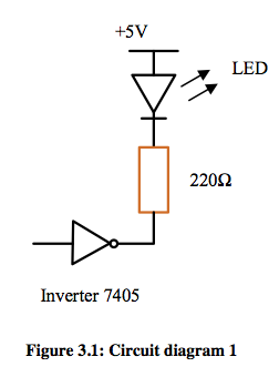
Use a simple wire as the input to your inverter. You should see the LED switch OFF when the wire is connected to the - ve ground supply (verify this).
2. Now construct the OR gate and the circuitry on the left-hand side of your breadboard, as shown in Figure 3.2. Take the output of the OR gate and input it into the inverter that you have placed on the right hand side as shown below.
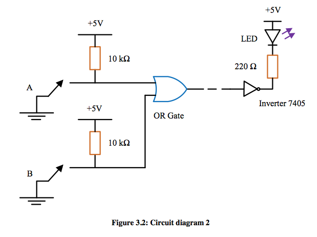
Operate the switches A & B independently.
Close the switches A & B and the LED should go out.
The LED should light if switches A or B are open, i.e. one or the other causes the LED to illuminate (verify this).
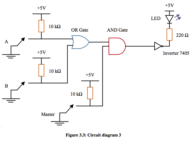
3. Construct the final part of the circuit, the AND gate, and connect it up as shown below in Figure 3.3.
The OR gate on the left-hand side of you breadboard, the AND in the centre and the INVERTER on the right. Ensure the output of the OR gate is connected to the input of the AND and the output of the AND is connected to the INVERTER. Now, your circuit should complete as shown in Figure 3.3 and the LED should illuminate.
Opening the switches A or B or both at the same time and the LED will remain off.
Now open the master switch and hold it in that position while opening switches A or B or both at the same time and the LED should be on.
- Aim
-