04
-
- Introduction
- ● So far we have taken a ‘black-box’ view of active components (such as op-amps)
● It is now time to look ‘inside the box’
– we will start by looking at diodes and semiconductors
– then progress to transistors
– later, we will look at more detailed aspects of circuit design
- Semiconductors and diodes
- ● Introduction
● Electrical properties of solids
● Semiconductors
● pn Junctions
● Diodes
● Semiconductor diodes
● Special-purpose diodes
● Diode circuits.
-
- Electrical properties of solids
- ● Conductors
– e.g. copper or aluminium
– have a cloud of free electrons (at all temperatures above absolute zero). If an electric field is applied electrons will flow causing an electric current
● Insulators
– e.g. polythene
– electrons are tightly bound to atoms, so, only a few can break free to conduct electricity
● Semiconductors
– e.g. silicon or germanium
– at very low temperatures these have the properties of insulators
– as the material warms up some electrons break free and can move about, and it takes on the properties of a conductor – albeit a poor one
– however, semiconductors have several properties that make them distinct from conductors and insulators
-
- Semiconductors
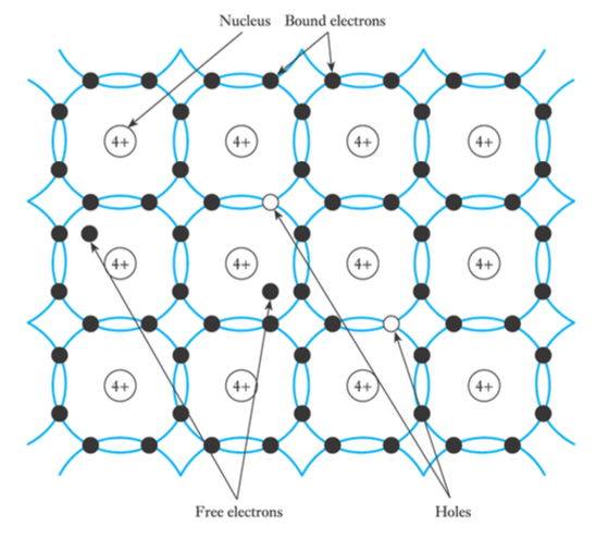
- ● Pure semiconductors
– thermal vibration results in some bonds being broken, generating free electrons which move about
– these leave behind holes which accept electrons from adjacent atoms and therefore, also move about
– electrons are negative charge carriers
– holes are positive charge carriers
● At room temperatures there are few charge carriers – pure semiconductors are poor conductors
– this is intrinsic conductionbr>
- Structure of a semiconductor
- ● The atomic structure of silicon
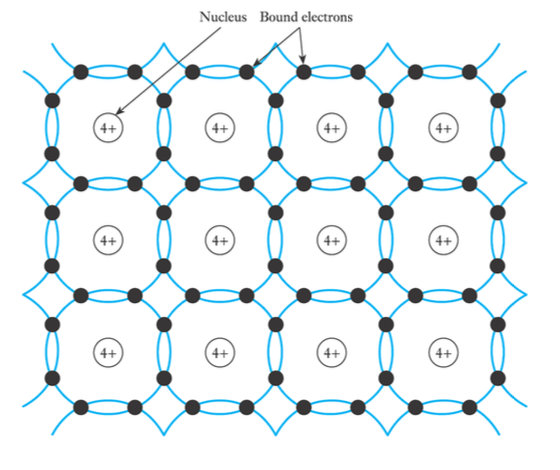
● The effect of thermal vibration on the structure of silicon
-
- Doping of semiconductors
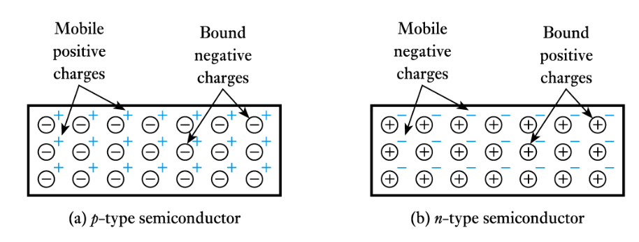
- ● Doping
– the addition of small amounts of impurities drastically affects its properties
– some materials form an excess of electrons and produce an n-type semiconductor
– some materials form an excess of holes and produce a p-type semiconductor
– both n-type and p-type materials have much greater conductivity than pure semiconductors
– this is extrinsic conduction
● The dominant charge carriers in a doped semiconductor (e.g. electrons in n-type material) are called majority charge carriers.
The other type are minority charge carriers
● The overall doped material is electrically neutral
-
- pn Junctions
- ● When p-type and n-type materials are joined, this forms a pn junction
– the majority charge carriers on each side diffuse across the junction where they combine with (and remove) the charge carriers of the opposite polarity
– hence, around the junction there are few free charge carriers and we have a depletion layer (also called a space charge layer)
● The diffusion of positive charge in one direction and negative charge in the other produces a charge imbalance – this results in a potential barrier across the junction
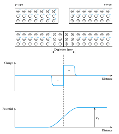
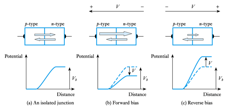
● Potential barrier
– the barrier opposes the flow of majority charge carriers and only a small number have enough energy to surmount it
• This generates a small diffusion current
– the barrier encourages the flow of minority carriers and any that come close to it will be swept over
• This generates a small drift current
– for an isolated junction these two currents must balance each other and the net current is zero
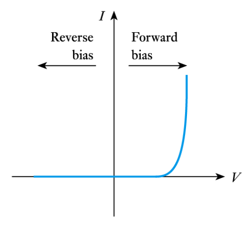
● Forward bias
– if the p-type side is made positive with respect to the n-type side the height of the barrier is reduced
– more majority charge carriers have sufficient energy to surmount it
– the diffusion current therefore increases while the drift current remains the same
– there is thus a net current flow across the junction which increases with the applied voltage
● Reverse bias
– if the p-type side is made negative with respect to the n-type side the height of the barrier is increased – the number of majority charge carriers that have sufficient energy to surmount it rapidly decreases – the diffusion current therefore vanishes while the drift current remains the same – thus the only current is a small leakage current caused by the (approximately constant) drift current – the leakage current is usually negligible (a few nA)
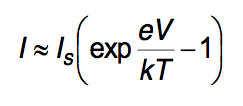
● Currents in a pn junction
● Forward and reverse currents
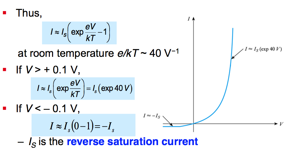
– pn junction current is given approximately by
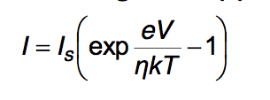
– where I is the current, e is the electronic charge, V is the applied voltage, k is Boltzmann’s constant, T is the absolute temperature and η (Greek letter eta) is a constant in the range 1 to 2 determined by the junction material
– for most purposes we can assume η =1
-
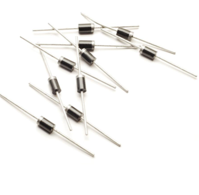
- Diodes
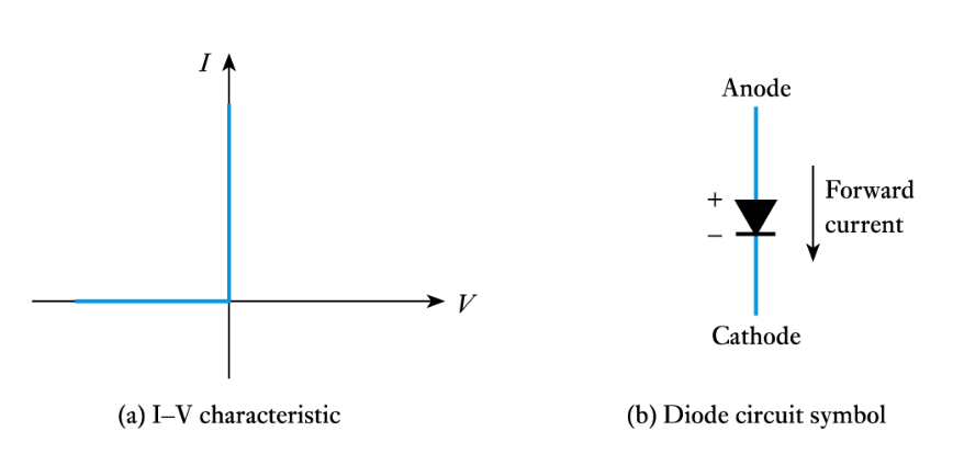
- ● An ideal diode passes electricity in one direction butnot in the other
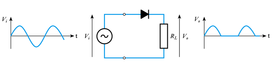
● One application of diodes is in rectification
– the example below shows a half-wave rectifier
● In practice, no real diode has ideal characteristics but semiconductor pn junctions make good diodes -
- Semiconductor diodes
- ● Forward and reverse currents
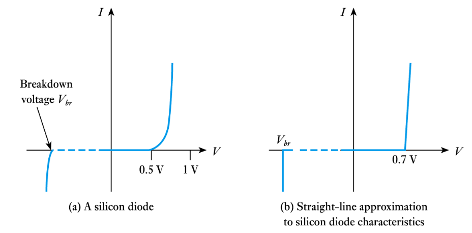
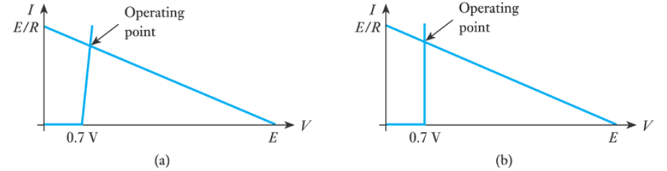
● Silicon diodes
– generally have a turn-on voltage of about 0.5 V
– generally have a conduction voltage of about 0.7 V
– have a breakdown voltage that depends on their construction
• perhaps 75 V for a small-signal diode
• perhaps 400 V for a power device – have a maximum current that depends on their construction
• perhaps 100 mA for a small-signal diode
• perhaps many amps for a power device
● Turn-on and breakdown voltages for a silicon device
- Diode circuit analysis
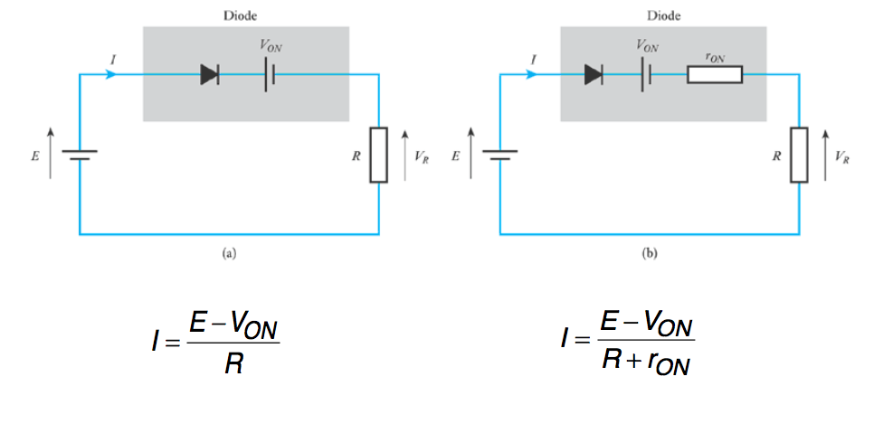
- ● The non-linear behaviour of diodes makes analysis difficult – consider this simple circuit
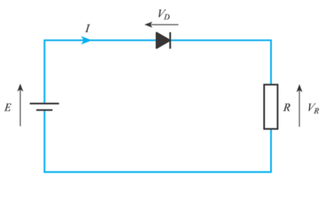
Applying Kirchoff’s voltage law
E=VD+VR
= VD+IR
From the diode equation
I=IS(exp40VD)
To find I we need to solve these two simultaneous equations
● One approach is through the use of a load line
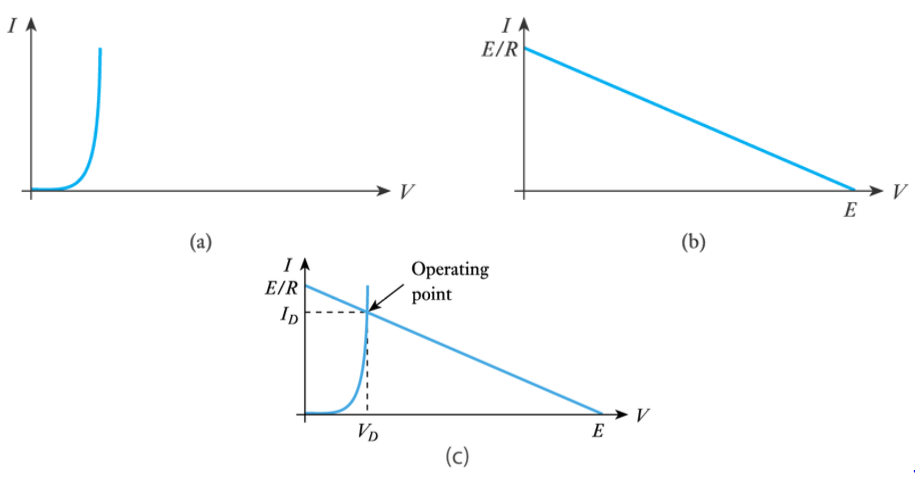
– Load lines can also be used with equivalent circuits...
...however, this is rarely done, since if an equivalent circuit is used, the circuit can normally be analysed directly, without resorting to a graphical method
-
- Reverse breakdown
- ● Can be caused by two mechanisms:
● Zener breakdown
– in devices with heavily doped p- and n-type regions the transition from one to the other is very abrupt
– this produces a very high field strength across the junction that can pull electrons from their covalent bonds.
– produces a large reverse current
– breakdown voltage is largely constant
– Zener breakdown normally occurs below 5 V
● Avalanche breakdown
– occurs in diodes with more lightly doped materials
– field strength across junction is insufficient to pull electrons from their atoms, but is sufficient to accelerate the electrons within the depletion layer
– they loose energy by colliding with atoms
– if they have sufficient energy they can liberate other electrons, leading to an avalanche effect
– usually occurs at voltages above 5 V
- Effects of temperature
- ● Earlier we noted that
– for a given I, the voltage is inversely proportional to T
– for a silicon diode, V decreases by about 2 mV per oC
– the diode current is also affected by the reverse saturation current, which increases with temperature
– IS increases by about 7% per oC
-
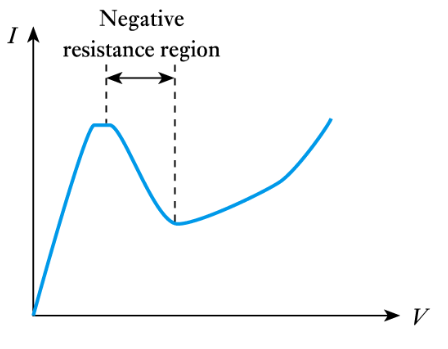
- ● Tunnel diodes
– high doping levels produce a very thin depletion layer which permits ‘tunnelling’ of charge carriers
– results in a characteristic with a negative resistance region
– used in high-frequency oscillators, where they can be used to ‘cancel out’ resistance in passive components
● Varactor diodes
– a reversed-biased diode has two conducting regions separated by an insulating depletion region
– this structure resembles a capacitor
– variations in the reverse-bias voltage change the width of the depletion layer and hence the capacitance
– this produces a voltage-dependent capacitor
– these are used in applications such as automatic tuning circuits
- Special-purpose diodes
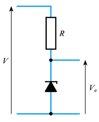 ● Zener diodes
– uses the relatively constant reverse breakdown voltage to produce a voltage reference
– breakdown voltage is called the Zener voltage, VZ
– output voltage of circuit shown is equal to VZ despite variations in input voltage V
– a resistor is used to limit the current in the diode
● Schottky diodes
– formed by the junction between a layer of metal
(e.g. aluminium) and a semiconductor
– action relies only on majority charge carriers
– much faster in operation than a pn junction diode
– has a low forward voltage drop of about 0.25 V
– used in the design of high-speed logic gates
- ● Tunnel diodes
-
- Diode circuits
- Watch this video 📹
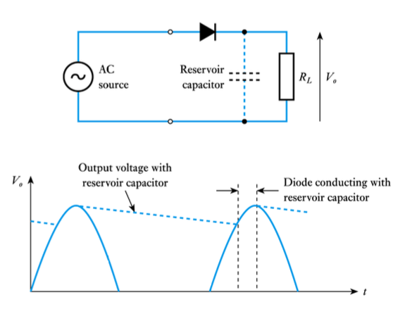
● Half-wave rectifier
– peak output voltage is equal to the peak input voltage minus the conduction voltage of the diode
– reservoir capacitor used to produce a steadier output
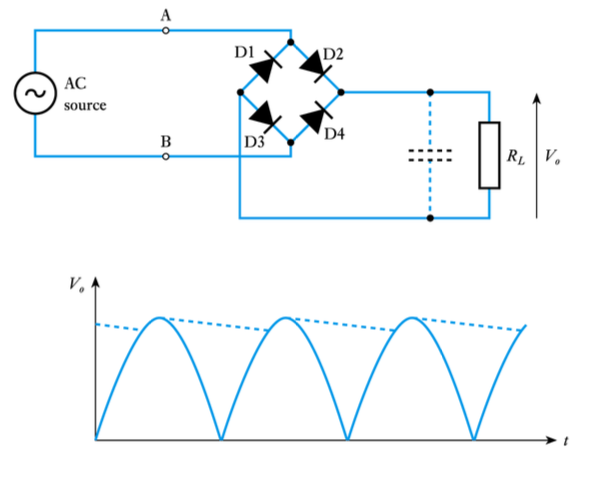
● Full-wave rectifier
– use of a diode bridge reduces the time for which the capacitor has to maintain the output voltage and thus reduce the ripple voltage
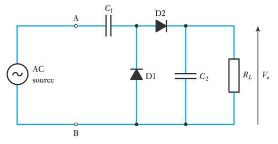
● Voltage doubler
– charges C2 to nearly twice the peak input voltage
– several stages can be cascaded to produce very high voltages
– ideal in applications requiring high voltages at low currents
Watch this video 📹
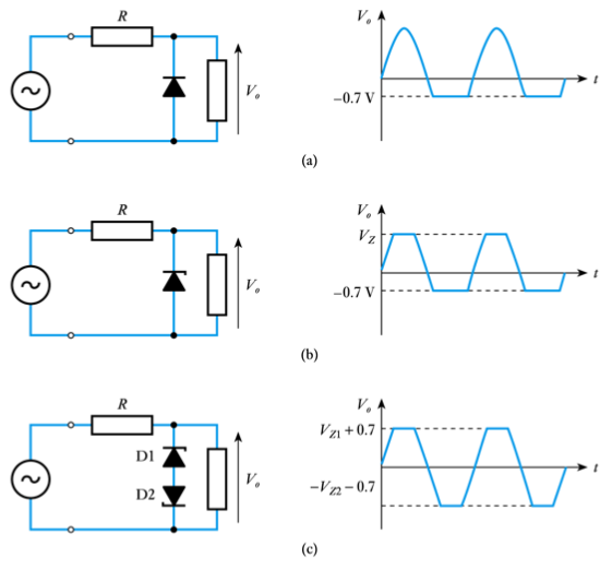
● Signal clamping
– a simple form of signal conditioning
– circuits limit the excursion of the voltage waveform
– can use a combination of signal and Zener diodes
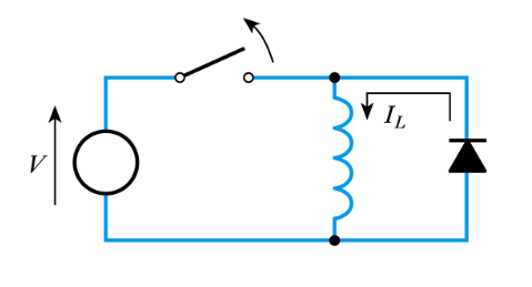
● Catch diode
– used when switching inductive loads
– the large back e.m.f. can cause problems such as arcing in switches
– catch diodes provide a low impedance path across the inductor to dissipate the stored energy
– the applied voltage reverse-biases the diode, which therefore has no effect
– when the voltage is removed the back e.m.f. forward biases the diode which then conducts
-
- Key points
● Diodes allow current to flow in only one direction
● At low temperatures semiconductors act like insulators
● At higher temperatures they begin to conduct
● Doping of semiconductors leads to the production of p-type and n-type materials
● A junction between p-type and n-type semiconductors has the properties of a diode
● Silicon semiconductor diodes approximate the behaviour of ideal diodes but have a conduction voltage of about 0.7 V
● There are also a wide range of special purpose diodes
● Diodes are used in a range of applications
- Further Study
● The Further Study section at the end of Chapter 17 is concerned with the design of a mains power supply.
● The supply is to drive an appliance that requires a fairly constant input of 12V and takes a current that varies from 100 to 200 mA.
● Design such a unit and then Watch this video 📹
-
-