05
-
- Introduction
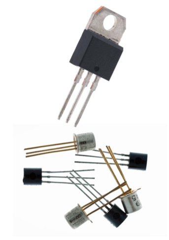
- ● Bipolar transistors are one of the main ‘building-blocks’ in electronic systems
● They are used in both analogue and digital circuits
● They incorporate two pn junctions and are sometimes known as bipolar junction transistors or BJTs
● Here will refer to them simply as bipolar transistors
- Bipolar junction transistors
 ● Introduction
● An overview of bipolar transistors
● Bipolar transistor operation
● A simple amplifier
● Bipolar transistor characteristics
● Bipolar amplifier circuits
● Bipolar transistor applications
● Circuit examples
-
- An overview of bipolar transistors
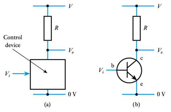
- ● Control in a bipolar transistor is generally considered to be due to an electric current
– Current into one terminal determines the current between two others
– A bipolar transistor can be used as a ‘control device’
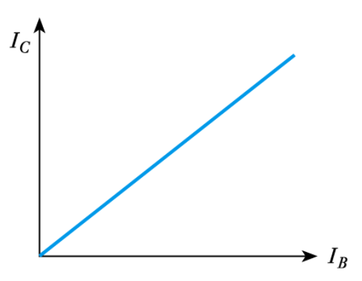
● Relationship between the collector current and the base current in a bipolar transistor
– characteristic is approximately linear
– magnitude of collector current is generally many times that of the base current
– the device provides current gain
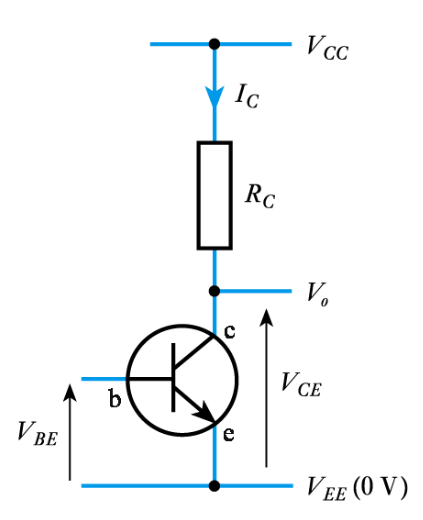
● Construction
– two polarities: npn and pnp
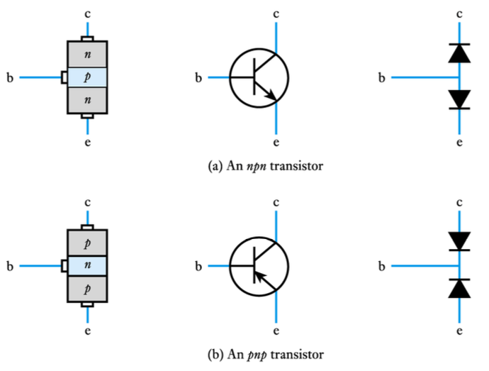
● Notation
– bipolar transistors are 3 terminal devices
• collector (c)
• base (b)
• emitter (e)
– the base is the control input
– diagram illustrates the notation used for labelling voltages and currents
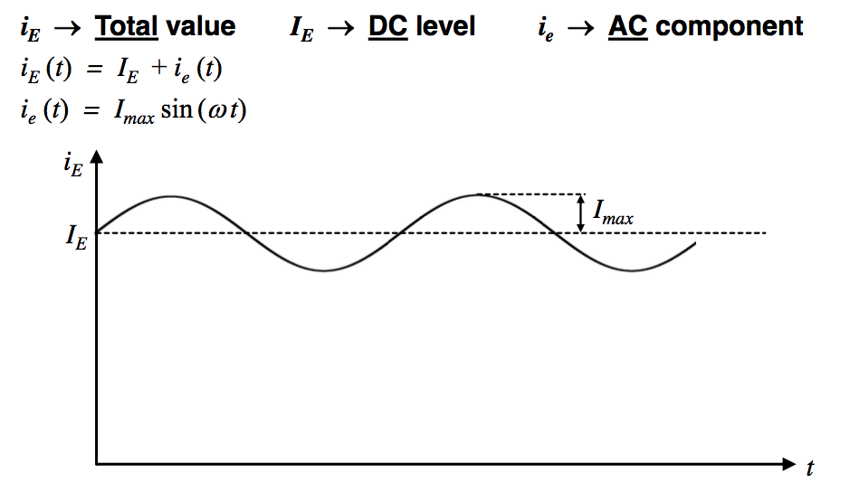
NOTATION
• In transistor circuits, voltages and currents have an AC component superimposed on a DC level.
• DC and AC voltages are analysed separately and independently • The following notation will be used (emitter current as example):
-
- Bipolar transistor operation
- ● We will consider npn transistors
– pnp devices are similar but with different polarities of voltage and currents
– when using npn transistors
• collector is normally more positive than the emitter
• VCE might be a few volts
• device resembles two back-to-back diodes – but has very different characteristics
• with the base open-circuit negligible current flows from the collector to the emitter
● Now consider what happens when a positive voltage is applied to the base (with respect to the emitter)
– This forward biases the base-emitter junction
– The base region is lightly doped and very thin
– Because it is lightly doped, the current produced is mainly electrons flowing from the emitter to the base
– Because the base region is thin, most of the electrons entering the base get swept across the base-collector junction into the collector
– This produces a collector current that is much larger than the base current – this gives current amplification
● Transistor action
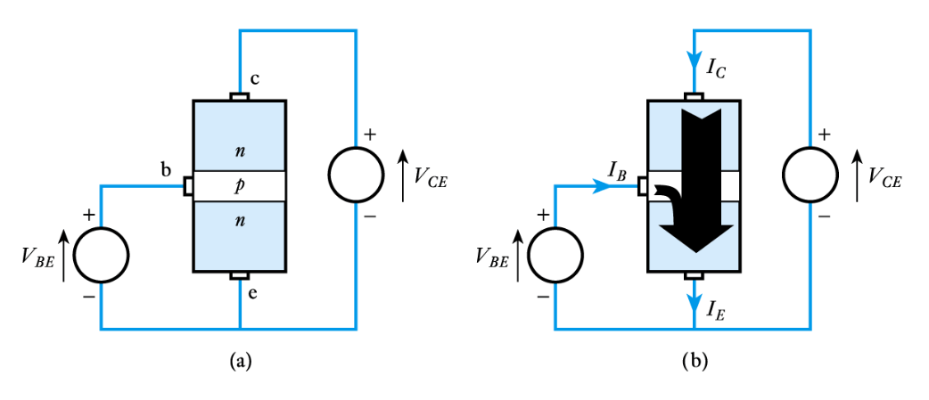
● Behaviour can be described by the current gain, hfe or by the transconductance, gm of the device
-
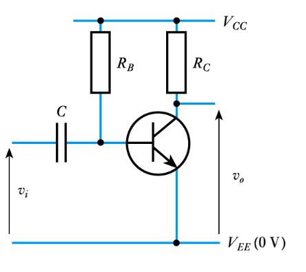
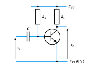
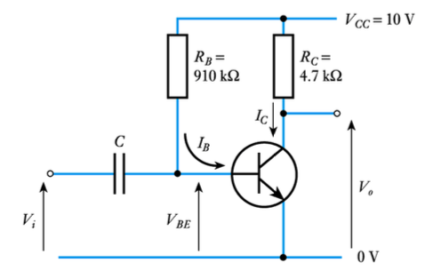
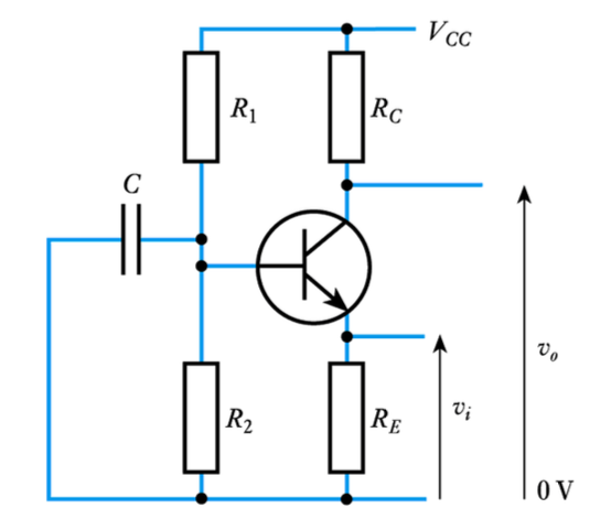
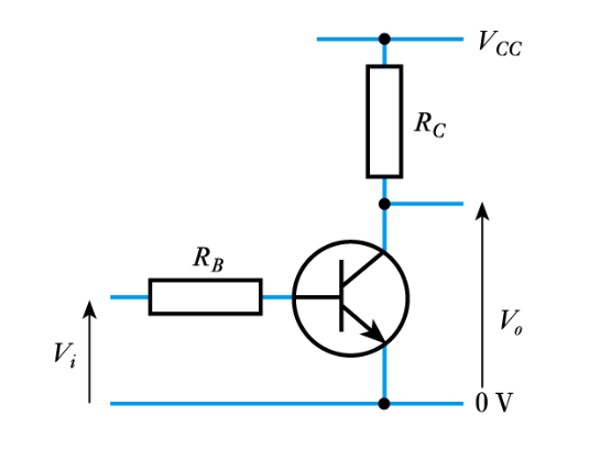
- A simple amplifier
Watch the Video 📹
● The circuit shows a simple amplifier
– RB is used to ‘bias’ the transistor by injecting an appropriate base current
– C is a coupling capacitor and is used to couple the AC signal while preventing external circuits from affecting the bias
– This is an AC-coupled amplifier
-
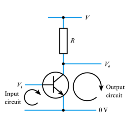
- Bipolar transistor characteristics
● Transistor configurations
– Transistors can be used in a number of configurations
– Most common is as shown
– Emitter terminal is common to input and output circuits
– This is a common-emitter configuration
– We will look at the characteristics of the device in this configuration
● Input characteristics
– The input takes the form of a forward- biased pn junction
– The input characteristics are therefore similar to those of a semiconductor diode
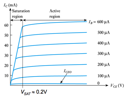
● Output characteristics
– region near to the origin is the saturation region
– this is normally avoided in linear circuits
– slope of lines represents the output resistance
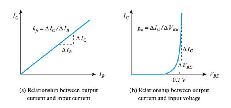
● Transfer characteristics
– can be described by either the current gain or by the transconductance
– DC current gain hFE or β is given by IC / IB
– AC current gain hfe is given by ic / ib
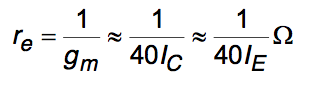
– transconductance gm is given approximately by
gm ≈ 40IC ≈ 40 IE siemens
– the units of gm are those of admittance
– therefore 1/gm has the units of resistance
– the quantity 1/gm is termed the emitter resistance re
– therefore
● Simple equivalent circuits for a bipolar transistor
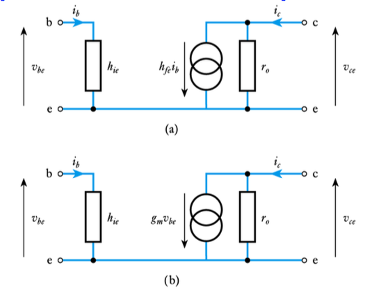
● Limitations of the simple models
– While the simple models shown above give a reasonable representation of the behaviour of devices they do not show the effects of the output voltage on the input (as shown here)
– This can be modelled by thereverse transfer ratio hre

● The hybrid-parameter model
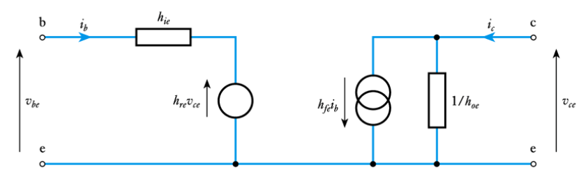
● The hybrid-Π model
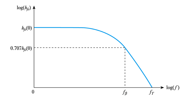
– gives a better representation at high frequencies

● Bipolar transistors at high frequencies
-
- Bipolar amplifier circuits
Watch the Video 📹
● Analysis of a simple amplifier
– Earlier we looked at a simple amplifier
– This is an AC-coupled amplifier
– It is convenient to look at its DC (or quiescent) behaviour separately from its AC (or small signal) behaviour
– We will begin by looking at its DC analysis
-
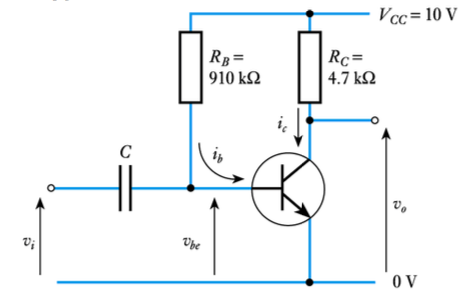
- ● Example (continued)
– The base-to-emitter voltage VBE is approximately 0.7 V.
– Therefore

- DC analysis of a simple amplifier
- ● Example – see Example 19.1 from course text
Determine the quiescent collector current and the quiescent output voltage of the following circuit, given that the hFE of the transistor is 100
- ● Example (continued)
-
- Small signal analysis of an amplifier
● To determine the small-signal behaviour of the circuit, we first construct a small-signal equivalent circuit
– We start with our model of the transistor
– Then add the other components
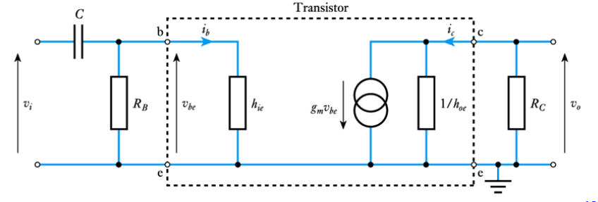
● From the equivalent circuit, if we ignore the effects of C
Vbe = Vi
and therefore
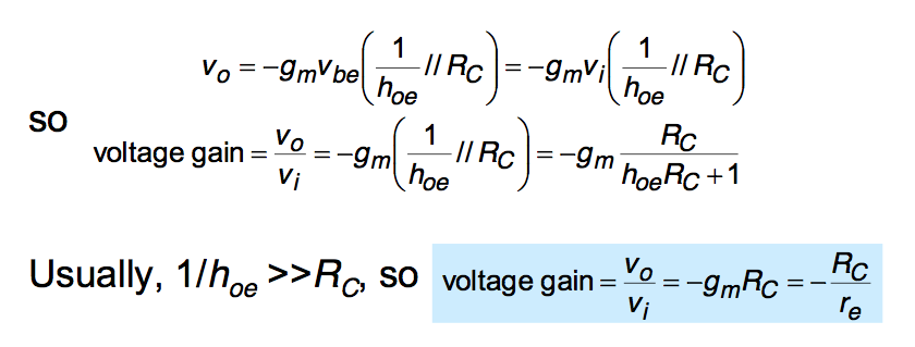
● Example – see Example 19.2 from course text
Determine the small signal voltage gain, input resistance and output resistance of the following circuit, given that hfe = 100 and hoe = 100 μS
The first step is to construct the small signal equivalent circuit
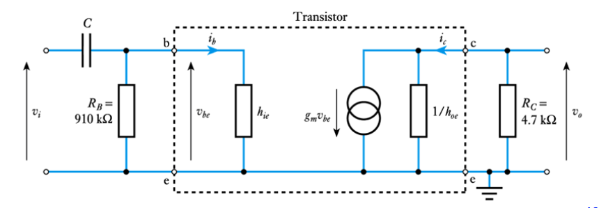
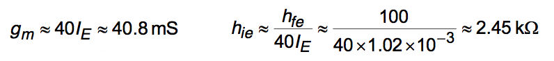
● We first need to establish gm and hie. From the earlier example IE ≈ IC = 1.02 mA Therefore
● Voltage gain

or, using the approximation: voltage gain ≈ -gm RC = -40.8x10-34700 ≈ -192
Given the inaccuracies involved, this seems a reasonable approximation
● Input resistance
– from the equivalent circuit the input resistance is simply RB // hie
– Since RC << 1/hoe then RC // (1/hoe) ≈ RC and therefore ro ≈ RC -
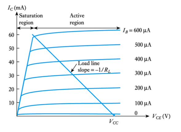
- Large signal considerations
- ● We can use a load line
- Choice of operating point
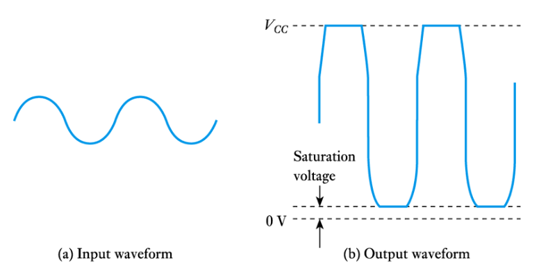
- ● There are several forbidden regions
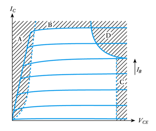
● Choice of operating point in a simple amplifier
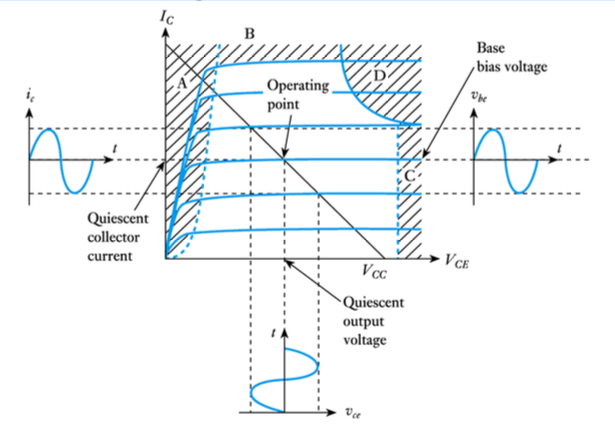
● Clipping of a sinusoidal signal
-
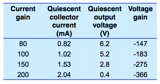
- The effects of device variability on amplifier characteristics
- ● Consider the effects of variations in the current gain of the transistor on the simple amplifier considered earlier
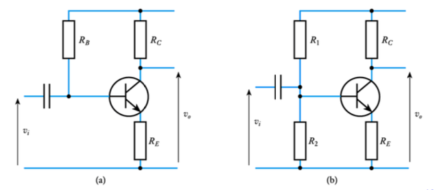
- The use of feedback
- Watch the Video 📹
● Feedback can be used to overcome the effects of device variability. Consider the following circuits
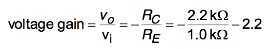
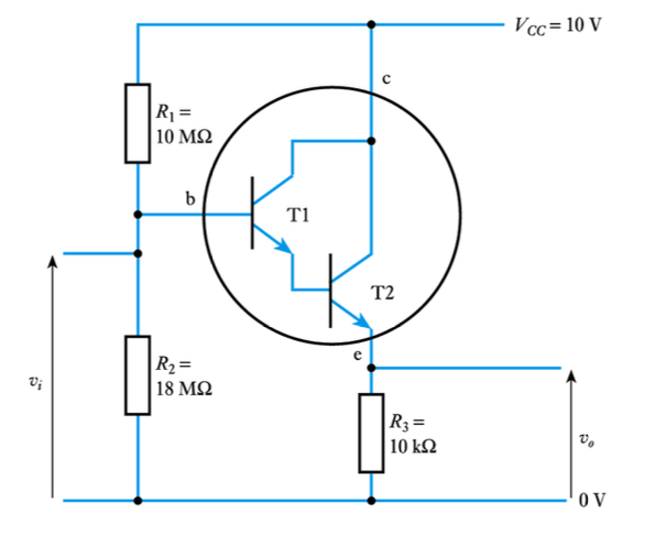
● Example – see Example 19.3 from course text Determine the quiescent voltages and currents in the following circuit
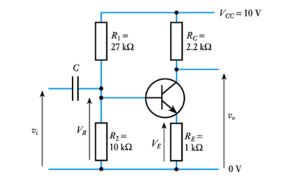
– If we assume that the basecurrent is negligible
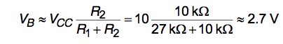
– Since VBE is approximately constant at about 0.7 V
V E = VB - VBE = 2.7 - 0.7 = 2.0V
– and
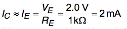
Vo(quiescent) ≈VC = VCC - IC RC = 10V - 2mA x 2.2kΩ = 5.6V
● Example – see Example 19.4 from course text Determine the small-signal behaviour of the following circuit

– If we assume that VBE is constant it follows that Vbe is very small, and Ve≈Vb≈Vi
– Therefore
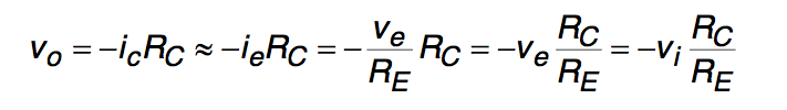
– and
-
- ● A comparison of the frequency responses of various amplifiers
– for simplicity, the figure shows the responses of amplifiers that are not fitted with coupling capacitors
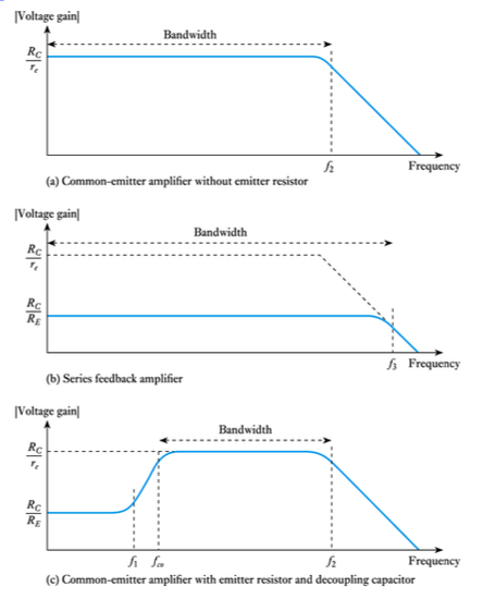
● Use of split emitter resistors
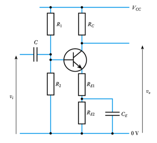
- Use of a decoupling capacitor
- ● A decoupling capacitor removes small-signal feedback
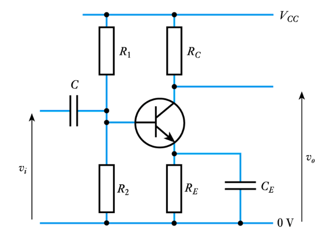
● Small-signal equivalent circuit of an amplifier using a decoupling capacitor

- ● A comparison of the frequency responses of various amplifiers
-
- Amplifier configurations
- ● So far we have concentrated on circuits where the input is applied to the base and the output is taken from the collector – the common-emitter amplifier is the simplest form of these
● Transistors are also used in other configurations
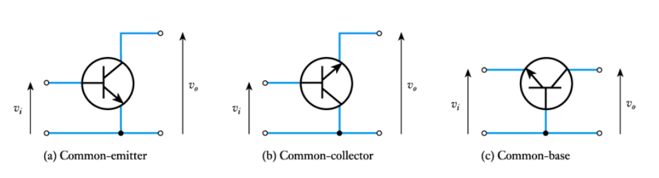
Watch the VIdeo 📹
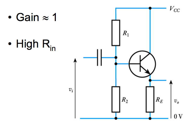
● A common-collector amplifier
● A common-base amplifier
-
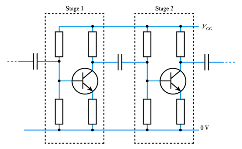
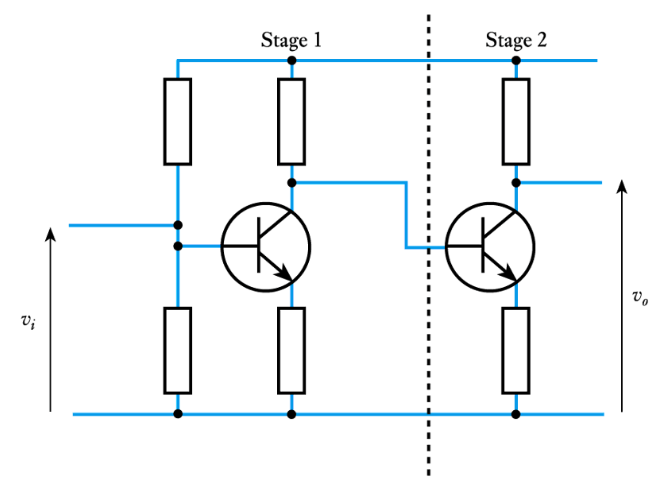
- Cascaded amplifiers
● Capacitive coupling between amplifier stages
- ● A two-stage DC-coupled amplifier
-
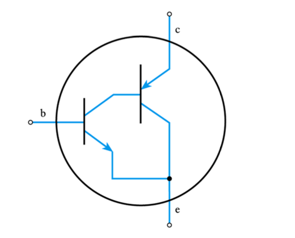
- Darlington transistors
- ● The darlington connection
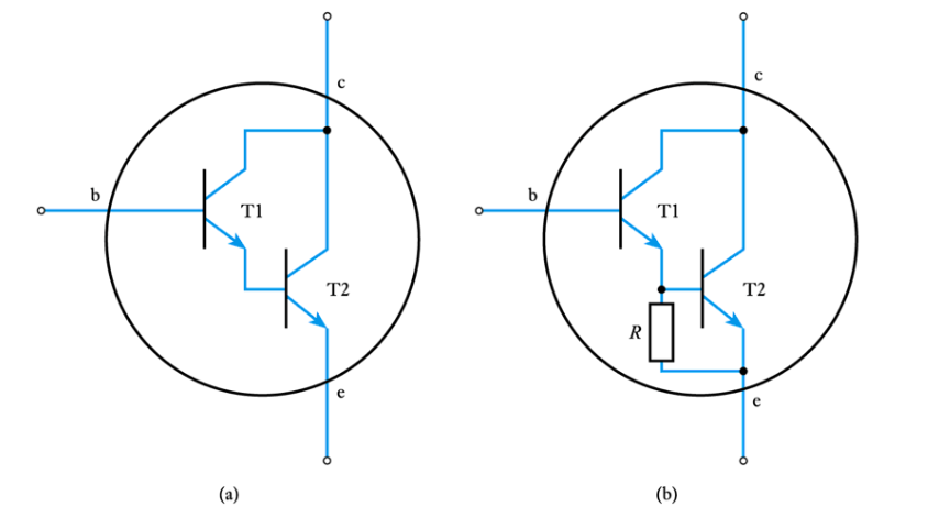
● A high input resistance buffer amplifier
● The complementary darlington connection
-
- Bipolar transistor applications
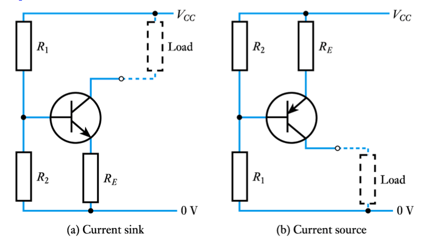
- ● A bipolar transistor as a constant current source
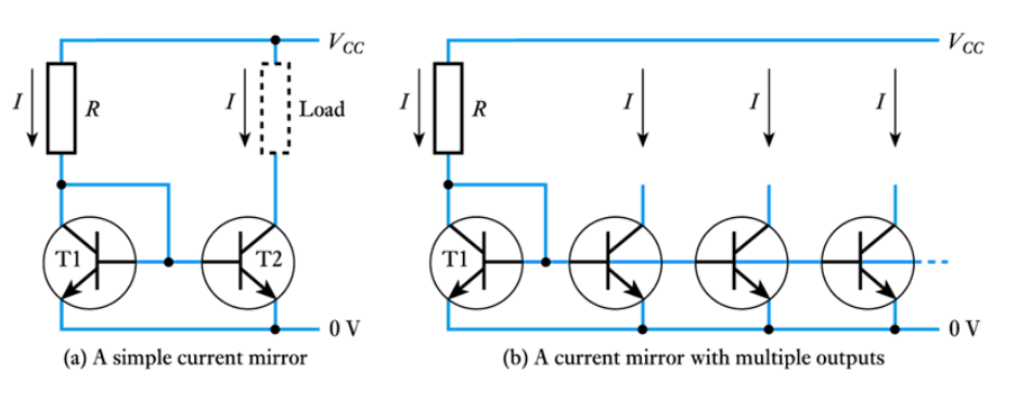
● A bipolar transistor as a current mirror
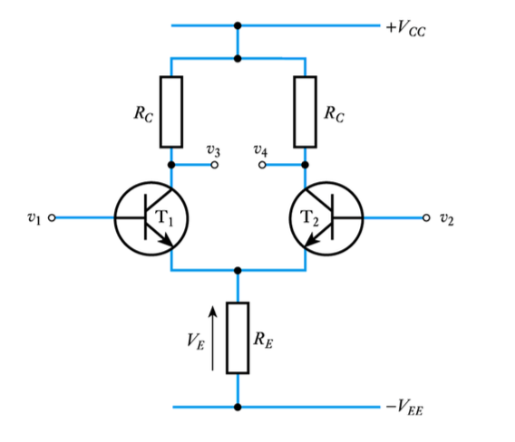
● Bipolar transistors as differential amplifiers
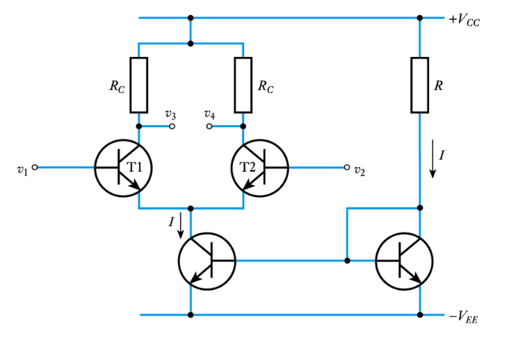
● A long-tailed pair amplifier using a current mirror
-
- Circuit examples
- ● A phase splitter

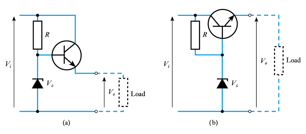
● A voltage regulator
● A logical switch
-
- Key points
- ● Bipolar transistors are widely used in both analogue and digital circuits
● They can be considered as either voltage-controlled or current-controlled devices
● Their characteristics may be described by their gain or by their transconductance
● Feedback can be used to overcome problems of variability
● Many amplifier circuits use transistors in a common-emitter configuration where the input is applied to the base and the output is taken from the collector
● Common-collector circuits make good buffer amplifiers
● Bipolar transistors are used in a wide range of applications
- Further Study
Watch the VIdeo 📹
● The Further Study section at the end of Chapter 19 looks at the design of a phase splitter.
● We considered a simple circuit earlier, but this suffers from the fact that its two outputs have very different output resistances.
● Design an arrangement to overcome this problem and then compare it with that shown in the video. -