06
-
- Introduction
- ● Field-effect transistors (FETs) are probably the simplest form of transistor
– widely used in both analogue and digital applications
– they are characterised by a very high input resistance and small physical size, and they can be used to form circuits with a low power consumption
– they are widely used in very large-scale integration
– two basic forms:
● insulated gate FETs
● junction gate FETs
- Field-effect transistors
- ● Introduction
● An overview of field-effect transistors
● Insulated-gate field-effect transistors
● Junction-gate field-effect transistors
● FET characteristics
● FET amplifiers
● Other FET applications
● FET circuit examples
-
- An overview of field-effect transistors
- ● Many forms, but basic operation is the same
– a voltage on a control input produces an electric field that affects the current between two other terminals
– when considering amplifiers we looked at a circuit using a ‘control device’
– a FET is a suitable control device
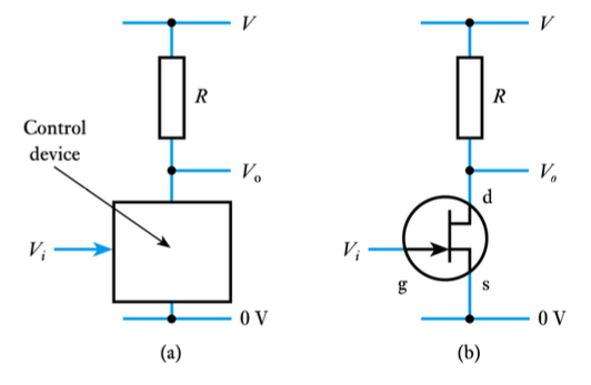
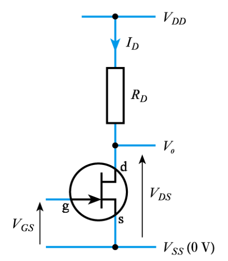
- ● Notation
– FETs are 3 terminal devices
● drain (d)
● source (s)
● gate (g)
– the gate is the control input
– diagram illustrates the notation used for labelling voltages and currents
-
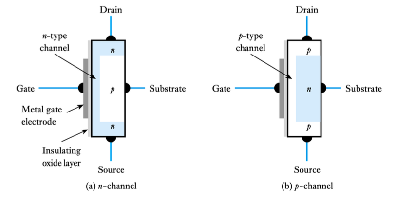
- Insulated-gate field-effect transistors
- ● Such devices are sometimes called IGFETs (insulated- gate field-effect transistors) or sometimes MOSFETs (metal oxide semiconductor field-effect transistors)
● Digital circuits constructed using these devices are usually described as using MOS technology
● Here we will describe them as MOSFETs
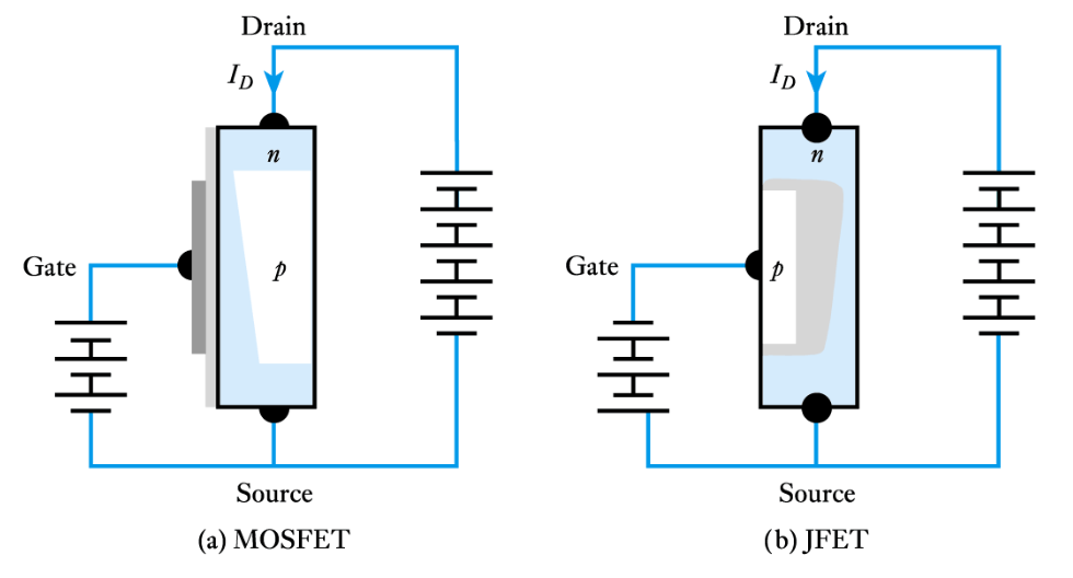
- MOSFET
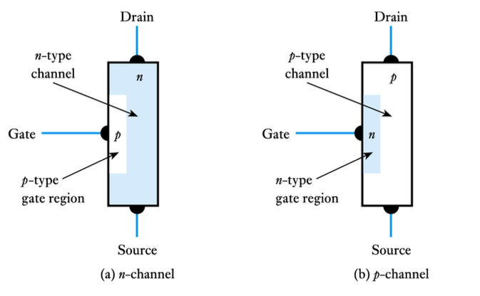
- ● Construction
– two polarities: n-channel and p-channel
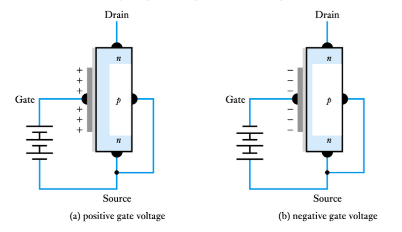
- ● Operation
– Gate voltage controls the thickness of the channel. – Consider an n-channel device
● making the gate more positive attracts electrons to the gate and makes the channel thicker – reducing the resistance of the channel. The channel is said to be enhanced
● making the gate more negative repels electrons from the gate and makes the channel thinner – increasing the resistance of the channel. The channel is said to be depleted
– The effect of varying the gate voltage
● Devices as described above are termed depletion- enhancement MOSFETs or simply DE MOSFETs
● Some MOSFETs are constructed so that in the absence of any gate voltage there is no channel
– Such devices can be operated in an enhancement mode, but not in a depletion mode (since there is no channel to deplete)
– These are called Enhancement MOSFETs
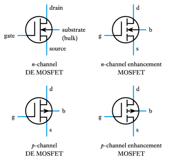
● Both forms of MOSFET are available as either
n-channel or p-channel devices
● MOSFET circuit symbols
-
- Junction-gate field-effect transistors
- ● Sometimes known as a JUGFET
● Here we will use another common name – the JFET
● Here the insulated gate of a MOSFET is replaced with a reverse-biased pn junction
● Since the gate junction is always reverse-biased no current flows into the gate and it acts as if it were insulated
- JFET
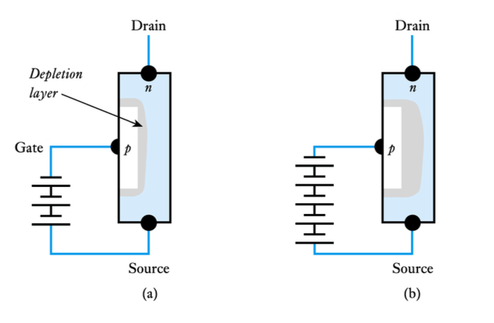
- ● Construction
– two polarities: n-channel and p-channel
● Operation
– The reverse-biased gate junction produces a depletion layer in the region of the channel
– The gate volt controls the thickness of the depletion layer and hence the thickness of the channel
– Consider an n-channel device
● the gate will always be negative with respect to the source to keep the junction between the gate and the channel reverse- biased
● making the gate more negative increases the thickness of the depletion layer, reducing the width of the channel – increasing the resistance of the channel
– the effect of varying the gate voltage
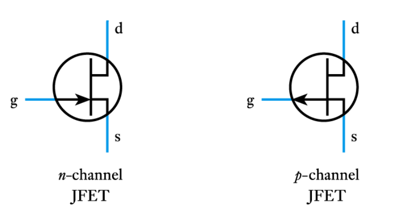
● JFET circuit symbols
-
- FET characteristics
- ● While MOSFETs and JFETs operate in different ways, their characteristics are quite similar
● Input characteristics
– in both MOSFETs and JFETs the gate is effectively insulated from the remainder of the device
● Output characteristics
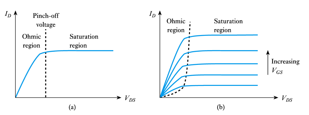
– consider n-channel devices
– usually the drain is more positive than the source
– the drain voltage affects the thickness of the channel
● FET output characteristics
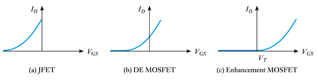
● Transfer characteristics
– similar shape for all forms of FET – but with a different offset
– not a linear response, but over a small region might be considered to approximate a linear response
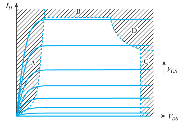
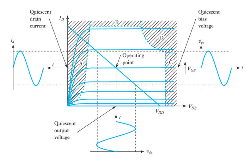
● Normal operating ranges for FETs
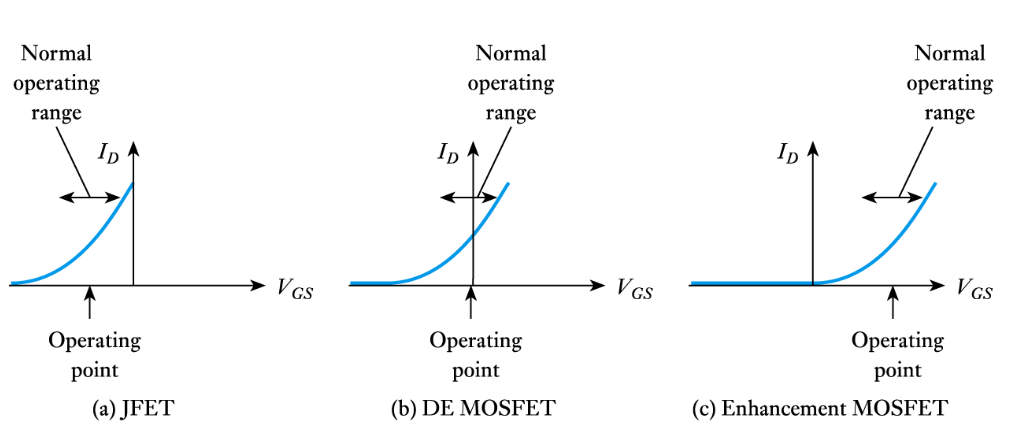
● When operating about its operating point we can describe the transfer characteristic by the change in output that is caused by a certain change in the input
– This corresponds to the slope of the earlier curves
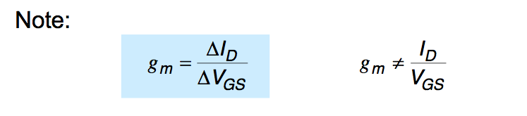
– This quantity has units of current/voltage, which is the reciprocal of resistance (that is conductance)
– Since this quantity describes the transfer characteristics it is called the transconductance, gm
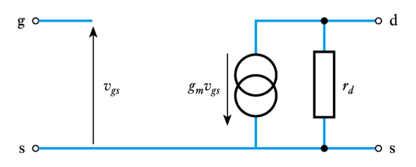
● Small-signal equivalent circuit of a FET
– models the behaviour of the device for small variations of the input about the operating point
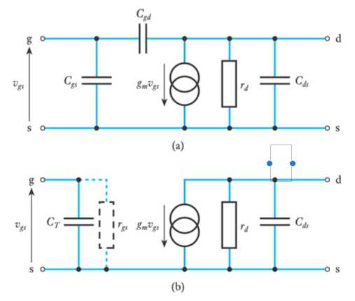
● FETs at high frequencies
– at high frequencies more sophisticated models are used
-
- FET amplifiers
- Watch the Video 📹
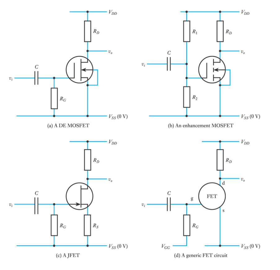
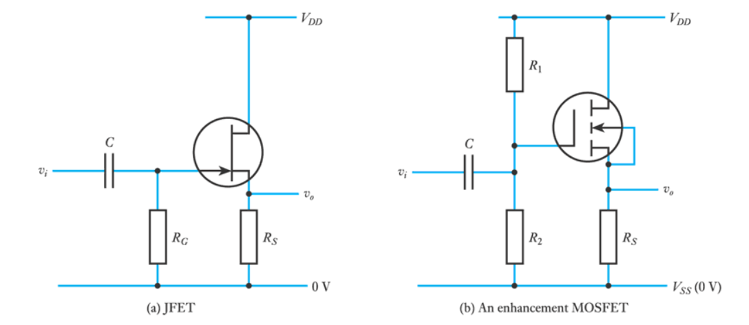
● Simple amplifiers can be formed using any kind of FET
– Figure (a) shows a circuit using a DE MOSFET
– Figure (b) uses an enhancement MOSFET
– Figure (c) uses a JFET
– Figure (d) is a generic circuit that could use any FET
– These are common source amplifiers
-
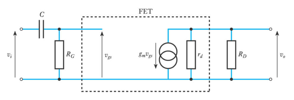
- Equivalent circuit of a FET amplifier
- Watch the Video 📹
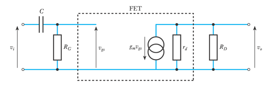
- ● This circuit can represent any of the FET amplifiers above (by choosing an appropriate value of RG)
– This is a small signal-equivalent circuit
– Note that RD goes to ground, since the supply voltage VDD is a virtual earth point for small signals
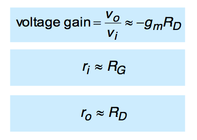
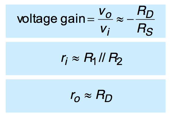
- Small-signal voltage gain
- ● From the equivalent circuit we can derive the small-signal voltage gain
v0= -gmvgs (rd//RD)
-gmvi (rd//RD)
therefore:
\frac{v_0}{v_i}= -g_m(r_d//R_D)
● Also
r_i\approx R_G r_0\approx r_d//R_D
● In many cases rd >>RD so rd can often be ignored
● If this is the case
-
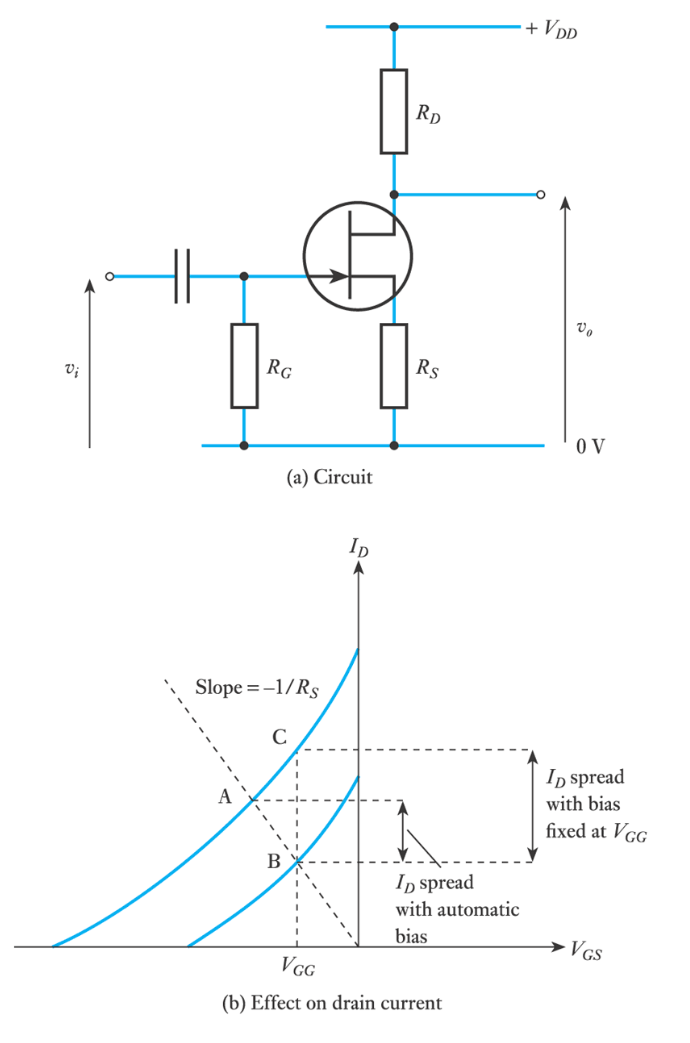
- Biasing considerations
- ● The biasing arrangement determines the operation of the circuit
– This is its quiescent state
● The quiescent output voltage vo(quies) is given by
V o(quies) = VDD -ID(quies)RD
● However, since the FET is not linear, determining the quiescent conditions is not straightforward
● One approach is to use a load line
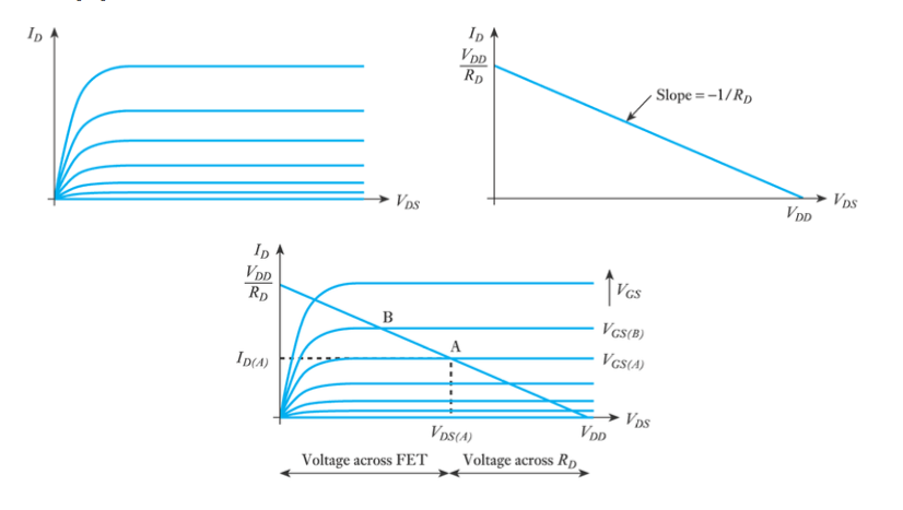
- Choice of operating point
- ● When selecting an operating point we need to avoid certain forbidden regions in the FET’s characteristics
- Device variability
- ● FETs, like all active devices, suffer from variability
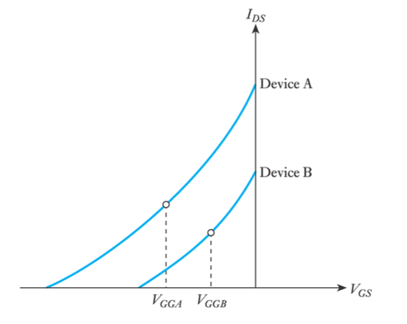
● The effects of device variability on the quiescent conditions of a circuit can be tackled using feedback
– for example, the use of ‘automatic’ bias
– see Examples 18.3 and 18.4 of the course text
-
- A negative feedback amplifier
- Watch the Video 📹
- ● Feedback can be used not only to stabilise the biasing conditions of a circuit, but also its voltage gain
● Analysis of this circuit (see text) shows that
– characteristics set by stable passive components
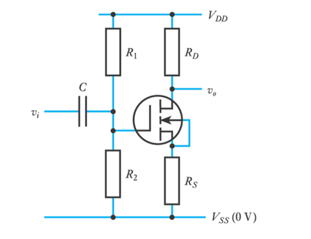
- Use of a decoupling capacitor
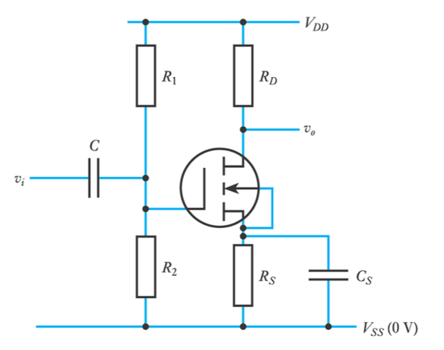
● The feedback amplifier has a relatively low gain
● Use of a decoupling capacitor can increase the gain by removing small-signal feedback
– Gain is similar to that of the common source amplifier
– Requires large CS at low frequencies
- Source followers
● These are unity-gain amplifiers with a low output resistance
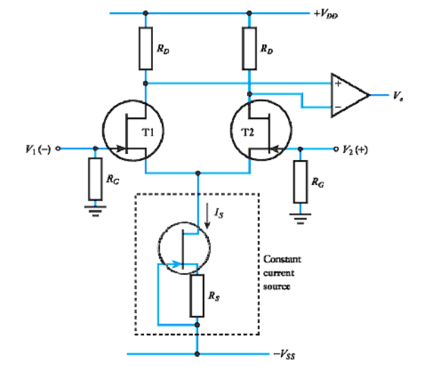
- Differential amplifiers
- ● A simple differential amplifier using JFETs – this is termed a long-tailed pair amplifier
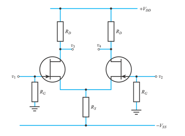
● Input voltage is vi = v1 - v2
● Output voltage is vo = v3 - v4
● Voltage gain is
= \frac{v_o}{v_i} = \frac{v_3 - v_4}{v_1 - v_2}\approx -g_mR_D
● CMRR is - CMRR≈ gmRS -
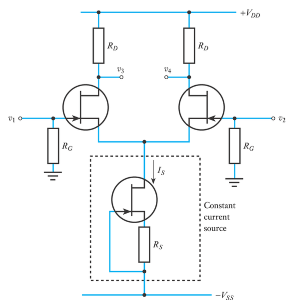
- Other FET applications
- ● FETs as constant current sources
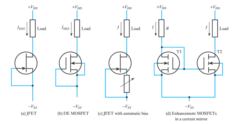
● A long-tailed pair amplifier with a FET current source
– the current source gives the effect of having a very high source resistor and therefore gives a very high CMRR
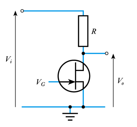
● A FET as a voltage-controlled resistance
– for small drain-to-source voltages FETs resemble voltage-controlled resistors
– the gate voltage VG is used to control this resistance
– can be used in a potential divider (as shown here) to produce a voltage-controlled attenuator
● A FET as an analogue switch
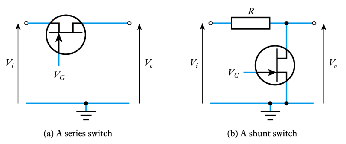
● A FET as a logical switch
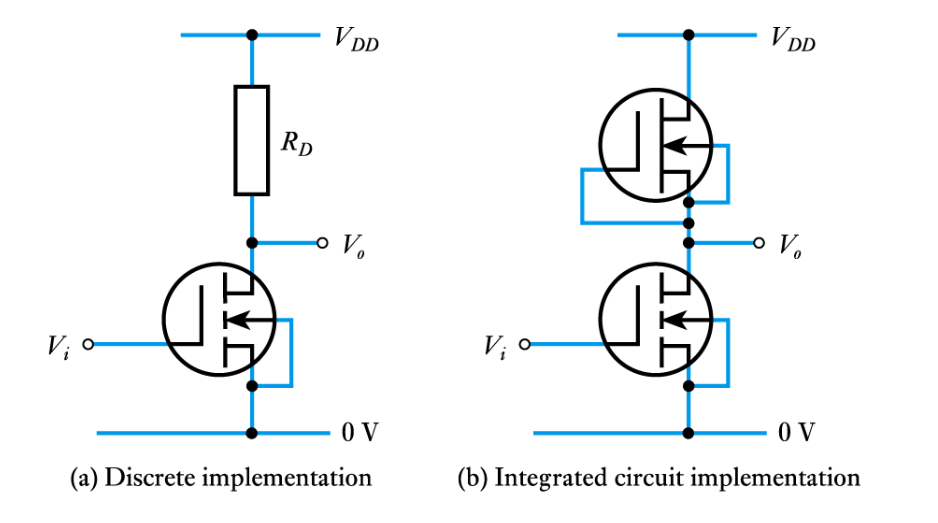
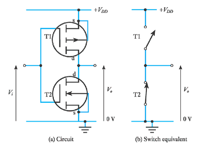
● CMOS circuits
– uses both p- and n-channel devices
– resembles two switches in series
– low output resistance in either state
-
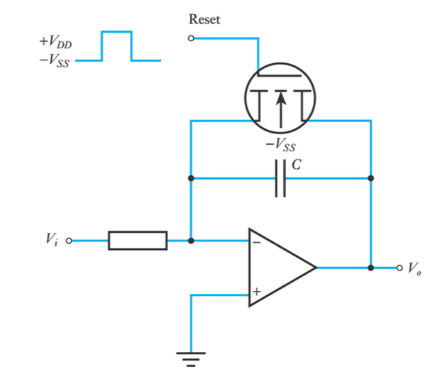
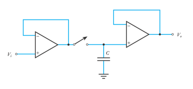
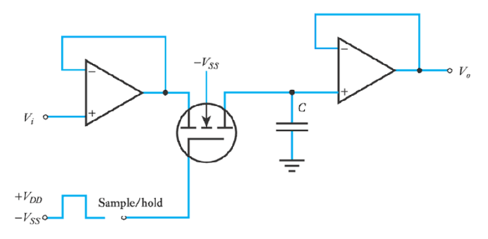
- FET circuit examples
- ● FET input buffer for an operational amplifier
- ● An integrator with reset
● A sample and hold gate – basic principle
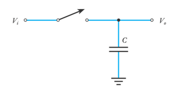
– gate with input and output buffers
● A FET sample and hold gate
-
- Key points
- ● FETs are widely used in both analogue and digital circuits
● They have high input resistance and small physical size
● There are two basic forms of FET: MOSFETs and JFETs
● MOSFETs may be divided into DE and Enhancement types
● In each case the gate voltage controls the current from the drain to the source
● The characteristics of the various forms of FET are similar except that they require different bias voltages
● FETs can be used in a range of amplifier configurations
● FETs can be also used to produce other circuit applications
-
-
-
- right
- left
-
- right