-
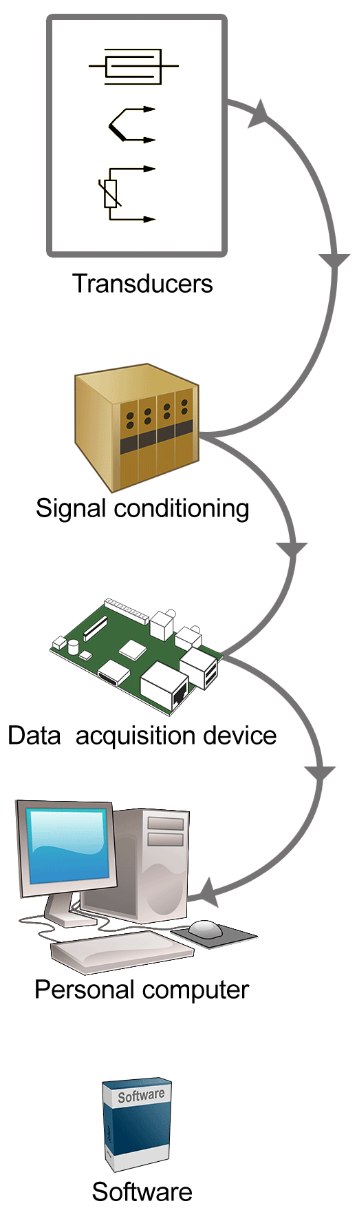 Figure 1 Typical PC Based DAQ System
Signal Conditioning and Real-Time Interfacing
Real-time interfacing is a general term used to describe the aspects of connecting a computer with a real-world process and communicating data between them in both ways. A Data Acquisition (DA) system is a collection of add-on hardware and software components that allow computer to receive real-world information from sensors. Although sensors can be based on electrical, mechanical, optical, or other principles, they all perform the same function: to convert real-world information (such as motion, temperature, and pressure) into low-power electrical signals which can be read by the computer. The current trend is to use personal computers (PCs) with DAQ hardware for data acquisition in areas of testing and measurement, industrial automation or laboratory research
The PC-based DAQ system depends on each of the following system elements. (Figure 1 opposite)
ComputerTransducers and sensorsSignal conditioningDAQ hardwareScrew terminal panel(s)General purpose input/output (GPIO) cardSoftware
-
Devices for Data Conversion
- The major components in the data conversion of the data from transducers are amplifiers, zero and span circuits and A/D and D/A converters. We will describe them in brief here.
Operational and Instrumentation Amplifiers
Operational Amplifiers
An amplifier is an electronic device which increases the size of volt- age or current signal without altering the signal’s basic characteristics. Operational amplifiers (op-amps) are termed operational because of their early growth in a computing area—mainly to perform mathematical operations. The operational amplifier has emerged as a basic building block in electronic circuits and is made up of many transistors fabricated on a processor chip. Its use arises from its ability to provide accurate and stable results under a wide range of operational conditions. Figure 2 is the schematic symbol for an operational amplifier showing its principle terminals. It is also characterized by very high gain, high input impedance, and very low output impedance. Without feedback, the amplifier would be unstable because of its excessive gain.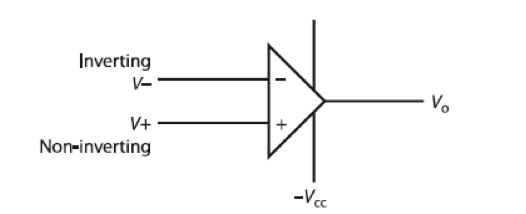 Figure 2. Schematic symbol of operational amplifier
The operational amplifier has three terminals known as the inverting input, non-inverting input, and the output. Depending on the magnitude of the components and the configuration used, differ- ent characteristics are obtained. Referring to Figure 2, the terminal identification is:
Vcc and -Vcc = power supply usually with magnitudes in the range of 10 to 15 V
V0 = output voltage terminal
V+ and -V- = input voltages
Thus,
A = voltage gain = $ \large \frac{V _{out}}{V _{in}} = \frac{V _0}{V_+ V _-} \small \rightarrow \infty $
R0 = output resistance (≈0)
Ri = input resistance (≈ $\infty$)
Basic characteristics of operational amplifier are:
(-) Inverting input terminal; A voltage applied to this terminal is amplified with an 180° phase shift.(+) Non-inverting terminal; A voltage applied to this terminal is amplified without a phase shift.The voltage gain is so great that the voltage difference between the inputs is zeroThe input impedance is so great that the inputs draw no current.Zero output impedance
From these parameters, the operating characteristics of the device are determined. For example, the infinite input resistance implies a zero input current at either input terminals:I+ = I- = 0Also, the zero output resistance implies that, regardless of the load on the output terminal, there will not be any loss in the output signal.
Continues on next tab
Transducers and Signal Conditioning
- Transducers sense physical phenomena and produce electrical signals that the DAQ system measures. For example, thermocouples, resistance temperature detectors (RTDs), thermistors, and IC sensors convert temperature into an analogue signal that an analogue-to-digital converter (ADC) can measure. The electrical signals generated by the transducers must be optimized for the input range of the DAQ device. Signal conditioning accessories amplify low-level signals and then isolate and filter them for more accurate measurements. In addition, some transducers use voltage or current excitation to generate a voltage output. The analogue input specifications give you information on both the capabilities and accuracy of the DAQ product. Basic specifications, which are available on most DAQ products, tell you the number of channels, the sampling rate, the resolution, and the input range.
- Amplification
The most common type of conditioning is amplification. For example, the low- level thermocouple signals should be amplified to increase the resolution and reduce noise. The signal should be amplified so that the maximum voltage range of the conditioned signal equals the maximum input range of the ADC.- Isolation
Another common signal-conditioning application is isolating the transducer signals from the computer for safety purposes. The system being monitored may contain high-voltage transients that could damage the computer without signal conditioning. Isolation ensures that the readings from the plug- in DAQ device are unaffected by differences in ground potentials or common-mode voltages. When the DAQ device input and the signal being acquired are each referenced to “ground,” problems occur if there is a potential difference in the two grounds. This difference can lead to ground loop, which may cause inaccurate representation of the acquired signal. If the difference is too large, it may damage the measurement system. Using isolated signal-conditioning modules eliminates ground loops and ensures that the signals are accurately acquired.- Multiplexing
A common technique for measuring several signals with a single measuring device is multiplexing. Signal-conditioning hardware for analogue signals often provides multiplexing for use with slowly changing signals like temperature. The ADC samples one channel, switches to the next channel, samples it, switches to the next channel, and so on. Because the same ADC samples many channels instead of one, the effective sampling rate of each individual channel is inversely proportional to the number of channels sampled.- Filtering
The purpose of a filter is to remove unwanted signals from the signal that you are trying to measure. A noise filter is used on DC-class signals, such as temperature, to attenuate higher frequency signals that can reduce the measurement accuracy. If the noise signals were not removed, they would erroneously appear as signals within the input bandwidth of the device. AC-class signals, such as vibration, often require a different type of filter known as an anti-aliasing filter. Like the noise filter, the anti-aliasing filter is also a low-pass filter; however, it requires a very steep cut- off rate, so it almost completely removes all signal frequencies that are higher than the input band- width of the device.- Excitation
Signal conditioning also generates excitation for some transducers. Strain gauges, thermistors, and RTDs (for example) require external voltage or current excitation signals. Signal-conditioning modules for these transducers usually provide these signals. RTD measurements are usually made with a current source that converts the variation in resistance to a measurable voltage. Strain gauges, which are very low-resistance devices, typically are used in a Wheatstone bridge con- figuration with a voltage excitation source.- Linearization
Another common signal-conditioning function is linearization. Many transducers, such as thermocouples, have a nonlinear response to changes in the phenomena being measured. Several software systems are available, including linearization routines for thermocouples, strain gauges, and RTDs.- Number of Channels
The number of analogue channel inputs is specified for both single-ended and differential inputs for devices with both input types. Single-ended inputs are all referenced to a common ground reference. These inputs typically are used when the input signals are high level (greater than 1 V), the leads from the signal source to the analogue input hardware are short (less than 5 m), and all input signals share a common ground reference. If the signals do not meet these criteria, you should use differential inputs. With differential inputs, each input has its own ground reference; noise errors are reduced because the common-mode noise is cancelled out.- Digital I/O
Digital I/O interfaces are often used on PC DAQ systems to control processes, generate patterns for testing, and communicate with peripheral equipment. In each case, the important parameters include the number of digital lines available, the rate at which you can accept and process digital data on these lines, and the drive capability of the lines. If the digital lines are used for controlling events (such as turning on and off heaters, motors, or lights), a high data rate is usually not required because the equipment cannot respond very quickly. The number of digital lines, of course, should match the number of processes to be controlled. In each of these examples, the amount of current required to turn the devices ON and OFF must be less than the available drive current from the device.
A common Digital I/O application is to transfer data between a computer and equipment sum as data loggers, data processors, and printers. Because this equipment usually transfers data in one byte (8- bit) increments, the digital lines on a plug-in DIO device are arranged in groups of eight. In addition, some boards with digital capabilities will have handshaking circuitry for communication- synchronization purposes. The number of channels, data rate, and handshaking capabilities are all- important specifications that should be understood and matched to the application needs. - The major components in the data conversion of the data from transducers are amplifiers, zero and span circuits and A/D and D/A converters. We will describe them in brief here.
-
(Cont.)- Another basic op-amp circuit is the inverting amplifier, as shown in Figure 6. The signal is applied to the inverting terminal through a resistor R1 with the non-inverting input connected to the ground. This results in an output that is out of phase with the input. A feedback path is provided from the output, through the resistor RF, and to the inverting input. It is to be noted that, since the + input terminal is at ground potential, then the - input terminal also must be at the ground; therefore,
V- = 0
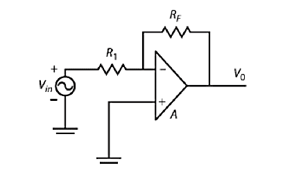 Figure 6. Inverting ampliefier
Since the voltage at the junction of the resistors R1 and RF = 0 and the input current to the op- amp is also 0, the currents in the resistors must be equal; therefore,
I1 = - I2$$ \frac{V_{in}}{R _1} = - \frac{V _0}{R_F} $$ Solving the last equation for output gives:
$$ V_0 = - \frac{R_F}{R_1} V_{in} $$ It can be noted that the closed-loop gain of the inverting amplifier depends only on the external resistors R1 and RF. Furthermore, the gain is negative (180° phase shift). This is an important difference between the inverting and non-inverting amplifiers. In the non-inverting configuration, the signal is applied to the op-amp input terminal, which has an infinite input resistance, and therefore, no current is drawn from the signal source. On the other hand, in the inverting amplifier, the signal is applied through the resistor combination, and as indicated above, a current is drawn from the source. For best results, it should be driven by a low output resistance source.
This current is: $$ I _{in} = \frac{V_{in}}{R_1} $$ From this, we may state:
Rin , non-inverting = $ \infty $
Rin , inverting = R1
This difference in the input resistance plays an important part in instrumentation amplifiers.
Continues on next tab
Operational and Instrumentation Amplifiers (Cont.)
- To study the effect of the infinite gain on operational amplifier, consider the circuit shown in Figure 3. Here the input voltage, Vin is actually equal to the difference between V+ and V-, between the input terminals. If Vin is varied over a wide range, the output voltage changes, as in Figure 3.
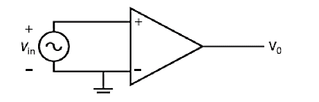 Figure 3. Test circuit for Op-Amp
In this example, a supply of ±15 V and an op-amp with a voltage gain equal to 200,000 is assumed. From the output characteristics in Figure 4, we see the output voltage never exceeds the power supply ±15 V. When operating in this region, the device is saturated. However, in the region between the two horizontal lines in the figure, the characteristics are very linear and have a slope equal to the gain (in this case 200,000). The main consideration here is the magnitude of input V voltage required to drive the operational amplifier into saturation, namely, either +75 or -75 μV. In other words, a voltage difference of 0.000075 V at the input terminals will cause the device to saturate. A very useful fact about operational amplifiers operating in their linear region is that the difference in potential across the input terminals approaches zero (due to the higher gain).
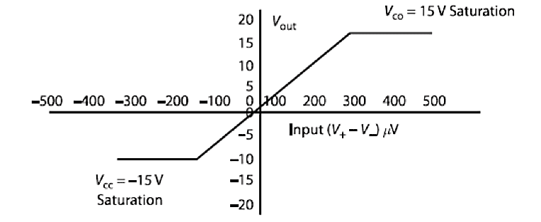 Figure 4. Op-Amp output characterstics
(V+ - V-) =0; V+ = V-
- Basic Op-Amp Circuits
As an example of a basic op-amp circuit, let us consider the non-invert- ing amplifier shown in Figure 5. It should be noted that the amplifier is non-inverting, because the sign of the output voltage relative to the ground is the same as the input voltage.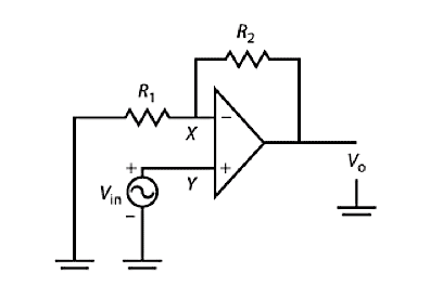 Figure 5. Non-inverting Amplifier
The output is considered to be taken from across a potential divider circuit consisting of R1 and R2 in series. The voltage Vx is a fraction of the output voltage: $$ V _- = \frac{R _2}{R _1 + R _2} V _0 $$ Since there is no current through the operational amplifier between the two inputs, there is no potential difference between them. Therefore,
Vx = Vin
From these two equation we can derive the output voltage:
$$ V _0 = \bigg( 1 + \frac{R _1}{R_2} \bigg) V _{in} $$ And this can be expressed as voltage gain:
$$ \frac{V_0}{V_{in}} = \bigg( 1 + \frac{R_1}{R_2} \bigg) $$ It can be noted that the closed-loop gain of the non-inverting amplifier depends only on the external resistors R1 and R2. Introducing the negative feedback through the resistors has reduced the overall closed-loop gain. While this feedback has reduced the gain, it has made the amplifier independent from the operation amplifier itself.
- Another basic op-amp circuit is the inverting amplifier, as shown in Figure 6. The signal is applied to the inverting terminal through a resistor R1 with the non-inverting input connected to the ground. This results in an output that is out of phase with the input. A feedback path is provided from the output, through the resistor RF, and to the inverting input. It is to be noted that, since the + input terminal is at ground potential, then the - input terminal also must be at the ground; therefore,
-
- Instrumentation Amplifier
The output signals of transducers are rarely at the levels required for the job at hand. The desired signal is often achieved using a versatile amplifier known as an instrumentation amplifier. The gain of this amplifier can be precisely set by the addition of a single external resistor, and it has a very high input resistance. It also has the ability to amplify small signals in the presence of noise. Figure 9 shows the schematic of an instrumentation amplifier.
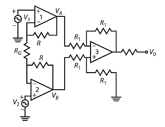 Figure 9. Instrumentation amplifier
In this configuration op-amp1 and op-amp2 are the input sections of the amplifier. Op-amp3 is a unity gain amplifier in the output section, which converts the output to the single end. The instrumentation amplifier shown in the figure has two inputs, which is useful for applications (such as strain gauge bridge circuits). The resistor RG is the external gain setting resistor. Letting V1 - V2 = Δ Vin and VA - VB = Δ Vo we can proceed with the following analysis:
Since the basic relation V+ = V- holds, the current through the gain setting resistor, RG, is $$ I _G = \frac{V _{A _{1}} - V _{B _{2}}}{R_G} = \frac{\Delta V_{in}}{R_G}$$ The input currents to the op-amps are zero; IG must flow through both resistors R and RG; therefore,
∆V0 = IR = $ \frac{\Delta V_{in}}{R_G} $ (2R + RG) = $ \bigg( 1+ \frac{ 2R}{ R_G} \bigg) \Delta V_{in}$This expression may be solved for the gain: $$ A = \bigg( 1+ \frac{2R}{R_G} \bigg) $$ In practice, the designer selects the value for R and the external resistor RG to suit the gain requirement. In addition to providing the gain necessary for a given application, most commercial instrumentation amplifiers also allow for zero setting. The characteristics of the instrumentation amplifier are high input resistance and their ability to amplify small signals in the presence of noise.
Amplifiers are susceptible to errors, such as nonlinearity errors, hysteresis errors and thermal stability errors. The three-op-amp configuration for instrumentation amplifiers is a popular design. Commercial units with these characteristics are available in the form of monolithic, modular single IC chips. Some models of instrumentation amplifiers are provided with power supply and digitally programmable resistor network units representing RG. Since the gain of these units can be changed in conjunction with data acquisition systems, they are known as programmable gain instrumentation amplifiers.
Operational and Instrumentation Amplifiers (Cont.)
- Zero and Span Circuits
Depending on specific applications, the output signals of transducers may need to be raised to the level needed. For example, consider a pressure sensor that has a sensitivity of 0.001 V/kPa over a range of 0 to 5000 kPa and has an output of 1.2 V at 0 kPa. If this sensor were used to measure a pressure of 0 to 1000 kPa and energize an A/D converter at voltage levels of 0-5 V, then some modification to the signal would be required. This situation is shown in Figure 7. In order to provide the desired signal for the A/D converter, the y-axis intercept and the slope of the sensor output are modified. For considering the slope, the output equation of the inverting amplifier is considered:
 Figure 7. (A) Transducer output, (B) A/D Input
$$ V_0 = - \bigg( \frac{R_F}{R_1} \bigg)$$ This equation is in the form: y = mx + b, (the equation for straight line), where the slope is the coefficient of the term on the right side is shown as:
Slope (span) = − $ \large \bigg( \frac{R_F}{R_1} \bigg)$
The b or y-intercept term can be obtained by adding a second input to the inverting amplifier as shown in Figure 8. Here VR is a constant reference voltage equal in magnitude to the y intercept. The output is obtained by considering each input separately and adding them. The result of this calculation is:
$$ V_0 = - \bigg( \frac{R_F}{R_1} \bigg) V_{in} - \bigg( \frac{R_F}{R_2} \bigg) V_R $$
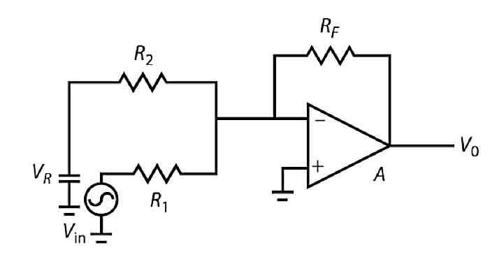 Figure 8. Multiple input inverting amplifier
The addition of the inverting amplifier with a gain of -1 will get rid of the negative output. The output expression for this amplifier is:
$$ V_0 = \bigg( \frac{R_F}{R_1} \bigg) V_{in} + \bigg( \frac{R_F}{R_2} \bigg) V_R $$
Question #1 - Signal Conditioning is normally performed on signals which are of following nature:
Question #2 - Instrumentation Amplifier, as presented in this lecture, can be used for linearization of non-linear response of some transducers:
- Instrumentation Amplifier
-
- Quantisation
Quantisation is a process of taking continuous analogue signals and breaking it into a number of discrete steps. The conversion is discrete and takes place one at a time. The A/D converter has two sides: one is the analogue side and the other is the digital side. The analogue-side specification includes a full-scale reference voltage range (VR). The A/D converter will operate under this range. The digital side is specified in terms of the number of bits of its register. A n-bit A/D converter will output n-bit binary numbers. The three functions of sampling, quantising, and encoding are involved in this process, which are shown in Figure 11.
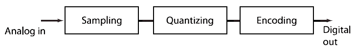 Figure 11. Functions of Analogue to Digital Conversion
The conversion process involves:
Sampling the continuous signalStoring this voltage, and, before the next sample is takenConverting the stored number to the binary number, which typically consists of a n-bit binary output word length
The quantization of a sampled analogue signal involves the assignment of a finite number of amplitude levels corresponding to discrete values of input signals VX between the range of 0 and the full-scale value of VR. If the A/D converter has a range of 10 bits, 1024 (210) different values of the input voltage can be represented. A typical voltage range for these systems is 10 V. Therefore, the resolution would be 10/1024 or about 10 mV, which yields about 0.1% accuracy.- Sampling Rate
This parameter determines how often conversions can take place. A faster sampling rate acquires more data in a given time and therefore often can form a better representation of the original signal.- Resolution
The number of bits that the ADC uses to represent the analogue signal is the resolution. The higher the resolution, the larger the number of divisions the range is broken into and, therefore, the smaller the detectable voltage change.
Figure 12 shows a sine wave and its corresponding digital image as obtained by an ideal 3-bit ADC. A 3-bit converter (as a simple example) divides the analogue range into 23, or eight divisions. Each division is represented by a binary code between 000 and 111. The resolution of the A/D converter is the number of bits used to digitally approximate the analogue value of the input. The number of possible states is equal to the number of bit combinations that results from the converter (which is equal to 2n, where n is the number of bits). Clearly, the digital representation is not a good representation of the original analogue signal, because information has been lost in the conversion.
By increasing the resolution to 16 bits, however, the number of codes from the ADC increases from 8 to 65536 to obtain an extremely accurate digital representation of the analogue signal.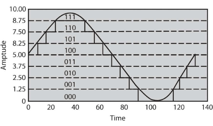 Figure 12. Digitised sine wave with a resolution of three bits
- The error that results from the quantisation process is called the quantisation error. The quantisation error can be as large as one-half the quantisation level spacing.
Quantisation error = ± ½
As a typical example, in a 8-bit A/D converter, the number of quantisation levels are 256 which is (28). For a maximum possible range of the voltage signal 0 to 10 V, the resolution is 10/256 or 0.0391 V, and the quantisation error = 0.0195 V. In the same way, a typical 12-bit A/D converter with a reference voltage of 10 V would be able to represent analogue voltages in the range between 0 and 10 V with 212 different binary values.
The main requirements for selecting an A/D converter include resolution, range of voltage needed, and speed of conversion.
Data Conversion Process
- Data acquisition systems in the real-time environment, especially using microcomputers, has become an important need in many automated manufacturing situations. If it is required to monitor several pieces of data at precisely the same time, sample and hold devices are necessary. A sample and hold device is used to hold each sampled value of the signal until the next pulse occurs.
In many mechatronic applications, the sensor signal is a complex, time-varying voltage that is considered a combination of many sine and cosine waves of different frequencies and amplitudes. A process of filtering eliminates some of the frequencies. Some of the sources of noise are the following:
Noises from the actuator motion, example being commutator brushes and relay contacts.Noise due to electromagnetic interference of transmission lines.Cross talk.
Filtering is used to remove certain band of frequencies from a signal, permitting others to be transmitted. A low-pass filter has a band, which allows all frequencies from zero to a certain level frequencies to be transmitted. A high-pass filter has a pass band, which allows all frequencies from a certain level up to infinity. A bandpass filter attenuates signals at both high and low frequencies and allows a range of frequencies to pass without attenuation.
In several cases, the computer reads the information from several channels one at a time using a device called multiplexer. The multiplexer is a switching device, which enables each of the inputs to be sampled in turn. It is a data selector that allows only one of the inputs to get through to the output. If it is necessary to control the experiment, the computer must supply the outputs in digital or analogue form. Data acquisition systems require the use of analogue-to-digital converters to input the sensed information coming from analogue transducers and sensors to computer system. Figure 10 shows a diagram of analogue-to-digital conversion using multiplexer, sample-and-hold circuits.
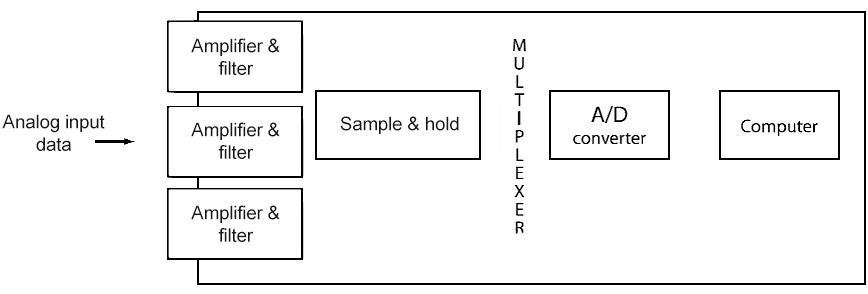 Figure 10. Multiplexer in an anologue-to-digital conversion environment
If the needed control signal is analogue (mainly for control valves and motors), digital output from the computer has to be processed through a digital-to-analogue converter. In a computer-aided process control system, the process control actions are recommended to the operator and displayed on the operator terminal. Automatic closed-loop process control systems require that the sensed data be manipulated to decide the control action, which should be subsequently and automatically implemented by means of suitable actuators. The majority of the actuators (other than stepping motors and relays) require analogue voltages and currents for their operation. It is therefore necessary to convert the digital binary output from the microcomputer into an analogue format.
The real-time interface handles the required digital data from the A/D or D/A converters. The control program is designed upon an overall analysis of the closed-loop control system. This control algorithm is executed during each sampling interval. If the bandwidth of the system is relatively high and multiple signals are sampled and converted, then efficient interface software is necessary.
Typical control programs can be generated in higher-level languages, in assembly level languages and in visual simulation languages. Assembly languages are useful in some instances where execution time is small and critical. Visual simulation procedures are used for situations where real-time data acquisition and control are done simultaneously using process models and sensor data. In these cases, block diagram-based models of manufacturing or industrial process are constructed and used in an atmosphere of hardware and software in one loop.
The Analogue-to-Digital Converter
- Although most of the sensors provide a direct signal output, a large number of transducers convert a dynamic variable into an analogue electric signal. It is necessary to use an analogue-to-digital converter (ADC) to transform an analogue voltage into a binary number through a process called quantization.
- Quantisation
-
(Cont.)
Flash type analogue-to-digital converters (as shown in Figure 14) are fast. The converter consists of a set of input comparators that act in parallel with each having an analogue input voltage as one input. The output of the latches is in digital form. The code converter consists of combinational logic circuits. For analogue input voltage, all of those comparators for which the analogue voltage is greater than the reference voltage will provide high output, and those for which it is less will provide low output.
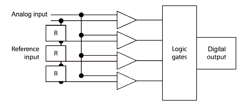 Figure 14. A/D conversion (Flash converter)
Digital-to-analogue converters reconstruct the digital signals into continuous-time analogue signals for the purpose of actuation and display. Some of the devices used in the mechatronic hardware area are analogue devices (such as solenoids or valves). To actuate these devices from a computer, the computer output signals have to be converted to analogue signals. A digital-to-analogue converter is similar to a digitally controlled potentiometer that is calibrated in the range of operation. The digital- to-analogue converters typically consist of a precise reference voltage, a weighed resistor network comprised of switches that can be closed or opened in response to changes in the digital code for the word, and an operational amplifier.
Digital-to-analogue conversion using software techniques involves the generation of a series of pulses by the microcomputer, which represents the digital information. The pulses are then applied to a resistor-capacitor network, which converts the digital data into an averaged DC signal. This software digital-to-analogue conversion technique has to be specially designed for high-speed applications. Monolithic single-chip digital-to-analogue converters, which use hardware to carry out high- speed conversion, are also used in control devices.
The Analogue-to-Digital Converter (Cont.)
- Conversion Resolution
The conversion resolution is identified smallest possible change as ΔV = VRx2-n (approximately) and is the smallest possible output voltage. For example, if 5 bits are used, the reference voltage is 10 V, ΔV = 10x2-5 = 0.3125 V/bit.- Range
Range refers to the minimum and maximum voltage levels that the ADC can quantise. DAQ devices offer selectable ranges, so the device is configurable to handle a variety of voltage levels. With this flexibility, you can match the signal range to that of the ADC to take advantage of the available measurement resolution.- Settling Time
Settling time is the time required for an amplifier, relays, or other circuits to reach a stable mode of operation. The instrumentation amplifier most likely will not settle when you are sampling several channels at high gains and high rates. Under such conditions, the instrumentation amplifier has difficulty tracking large voltage differences that can occur as the multiplexer switches between input signals. Typically, the higher the gain and the faster the channel switching time, the less likely the instrumentation amplifier is to settle.- Noise
Any unwanted signal that appears in the digitized signal of the DAQ device is noise. Because the PC is a noisy digital environment, acquiring data on a plug-in device takes a careful layout on multiple-layer DAQ devices by skilled analogue designers. Simply placing an ADC, instrumentation amplifier, and bus interface circuitry on a one or two-layer board will likely result in a very noisy device. Designers can use metal shielding on a DAQ device to help reduce noise. Proper shielding not only should be added around sensitive analogue sections on a DAQ device but also must be built into the layers of the device with ground planes.- Triggers
Many DAQ applications need to start or stop a DAQ operation based on an external event. Digital triggers synchronize the acquisition and voltage generation to an external digital pulse. Analogue triggers, used primarily in analogue input operations, start or stop the DAQ operation when an input signal reaches a specified analogue voltage level and slope polarity.
Successive Approximation Type of A/D Converter
- The successive approximation type of A/D converter (as displayed in Figure 13) is a popular type of A/D converter. It uses a trial-and-error approach to estimate the input voltage to the A/D, which needs conversion. The pulses generated by the output of the clock are counted in a binary manner. A D/A converter changes it to analogue voltage. A voltage comparator compares the clock-generated voltage to the input analogue voltage of the sensor. In this type of A/D converter, a series of known analogue voltages are generated and compared to the input voltage. When the analogue input from the sensor equals the clock-generated voltage, the pulses from the clock are stopped. The counter output represents the digital equivalent of the analogue input from the sensor.
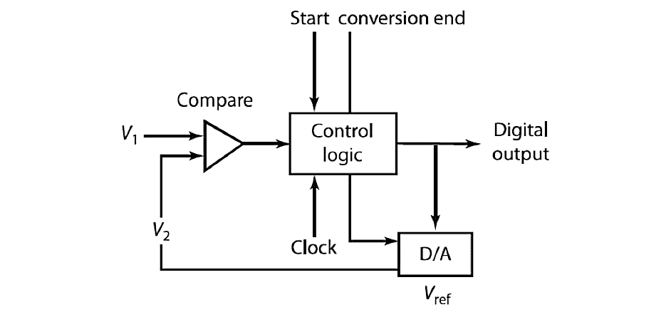 Figure 13. A/D Conversion (Successive Approximation Conversion)
Question #1 - The amount of digital data generated in Digital Conversion process depends on:
Question #2 - Quantisation is fully reversible process: