-
-
Introduction to Power Electronics + Devices
Power Electronics is a field which combines Power (electric power), Electronics and Control systems.
Power engineering deals with the static and rotating power equipment for the generation, transmission and distribution of electric power.
Electronics deals with the study of solid state semiconductor power devices and circuits for Power conversion to meet the desired control objectives (to control the output voltage and output power).Thus, Power electronics may be defined as the subject of applications of solid state power semiconductor devices (Thyristors) for the control and conversion of electric power. Power electronics deals with the study and design of Thyristorized power controllers for variety of application like Heat control, Light/Illumination control, Motor control - AC/DC motor drives used in industries, High voltage power supplies, Vehicle propulsion systems, High voltage direct current (HVDC) transmission.
Brief history of power electronics
The first Power Electronic Device developed was the Mercury Arc Rectifier during the year 1900. Then the other Power devices like metal tank rectifier, grid controlled vacuum tube rectifier, ignitron, phanotron, thyratron and magnetic amplifier, were developed & used gradually for power control applications until 1950.
The first SCR (silicon controlled rectifier) or Thyristor was invented and developed by Bell Lab's in 1956 which was the first PNPN triggering transistor. The second electronic revolution began in the year 1958 with the development of the commercial grade Thyristor by the General Electric Company (GE). Thus the new era of power electronics was born. After that many different types of power semiconductor devices & power conversion techniques have been introduced. The power electronics revolution is giving us the ability to convert, shape and control large amounts of power.
-
What is Power Electronics?
Power Electronics: is the application of electronic circuits to the control and conversion of electrical energy.
Where can we find Power Electronics?
COMMERCIAL and INDUSTRIAL APPLICATIONS
Heating Systems Ventilating, Air Conditioners, Central Refrigeration, Lighting, Computers and Office equipments, Uninterruptible Power Supplies (UPS).
DOMESTIC APPLICATIONS
Cooking Equipments, Lighting, Heating, Air Conditioners, Refrigerators & Freezers, Personal Computers, Entertainment Equipments, UPS.
TELECOMMUNICATIONS
Battery chargers, power supplies (DC and UPS), mobile cell phone battery chargers.
TRANSPORTATION
Traction control of electric vehicles, battery chargers for electric vehicles, electric locomotives, street cars, trolley buses, automobile electronics including engine controls. -
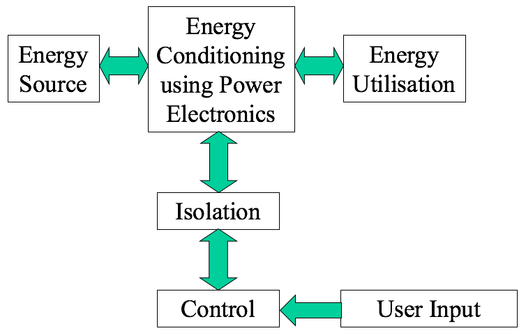
Basic Principles
- Power electronic circuits use switches.
- An ideal switch controls energy flow without any loss.
- In power electronics, we study how to operate and control switches to convert energy in the desired way.
- For this reason, we usually start the study of power electronic systems by studying the devices used as switches, their characteristics, theory of operation and control.
- Following this comes the use of these devices to convert energy according to different supply and load conditions.
-
Devices
- Silicon Controlled Rectifier
- Diode
-Thyristor
-Gate Turn off Thyristor (GTO)
-Triac
- Transistors
- Bipolar Junction Transistor (BJT)
- Metal Oxide Field Effect Transistor (MOSFET)
- Insulated Gate Bipolar Junction Transistor (IGBT)
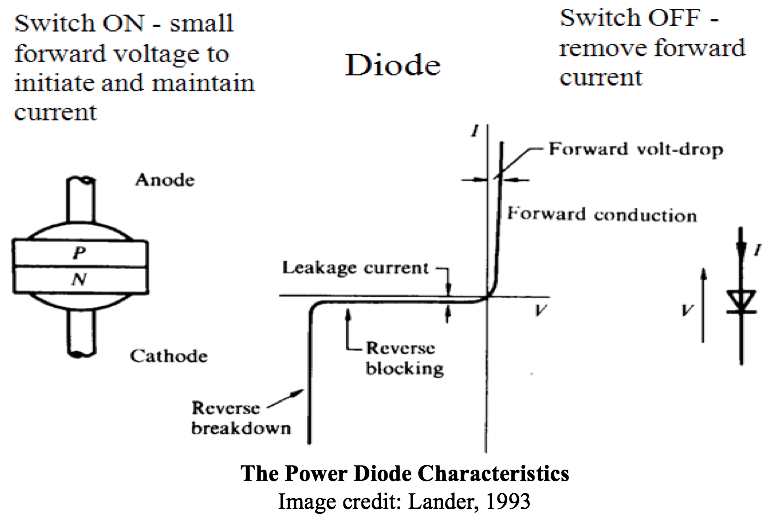
The Power Diode
- Power diode consists of a p-n junction similar to low power diodes
- Able to handle much higher currents.
The Thyristor
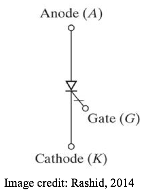
- The thyristor is a 3-terminal, 3-junction, 4-layer device made of alternate layers of p and n type silicon.
- The end p type region is the anode, the end n type region is the cathode and the inner p type region is the gate.
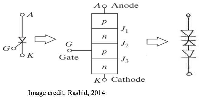
- Silicon Controlled Rectifier
-
The Thyristor Characteristics
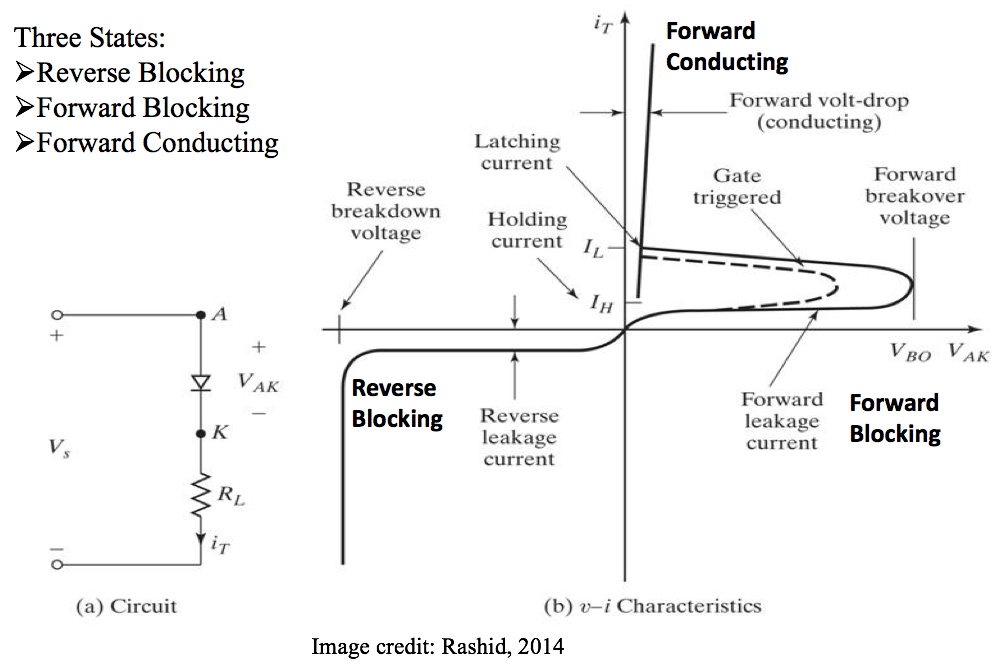
When the anode voltage is positive with respect to the cathode, only a small leakage current flows from anode to cathode. The thyristor is in the forward blocking, or off-state, condition and the leakage current is known as off-state current, ID.
If VAK is increased to a large value, the reverse-biased junction breaks. This is known as avalanche breakdown and the corresponding voltage is called forward breakdown voltage VBO. The device is in a conducting state, or on-state and large forward current flows limited by an external impedance. The anode current must be more than latching current IL to maintain current flow, otherwise, the device reverts to the blocking. This method of turn ON is avoided in practice as it can destroy the device.
Latching current IL is the minimum anode current to switch the thyristor on, after the gate signal has been removed.
Once a thyristor conducts, it behaves like a conducting diode and there is no control over the device. However, if the forward anode current is reduced below a level known as the holding current IH, the device turns off. The holding current is in the order of mA and is less than the latching current IL. Holding current IH is the minimum anode current to keep the thyristor ON.
While the thyristor conducts, the voltage drop between the anode and the cathode is about 1 to 2V
When the cathode voltage is positive with respect to the anode, the thyristor is in the reverse blocking state and a reverse leakage current, known as reverse current IR, flows through the device.
The Thyristor switch on/off conditions
- Switch ON
- apply forward voltage to anode/cathode
- apply current to gate (+ve gate/cathode)
- resultant anode/cathode current to exceed latching current of device
- gate current can be removed
- stays on provided anode/cathode sustained in forward direction (> holding value for device)
- Switch OFF
- Anode/cathode current reduced to less than holding current
- by forced commutation (dc system)
- by natural commutation (ac system)
- Blocks in reverse direction up to breakdown voltage.
The Gate Turn-off Thyristor (GTO)
The gate turn-off thyristor is a three terminal pnpn device similar in construction and performance to the conventional thyristor. Like thyristor, the GTO can be turned on by +ve gate current, but it can also be turned off by –ve gate current.
- Switch ON
-
The Triac
The Triac is a five-layer device, having a pnpn path in either direction between terminals T1 and T2 and can conduct in either direction.
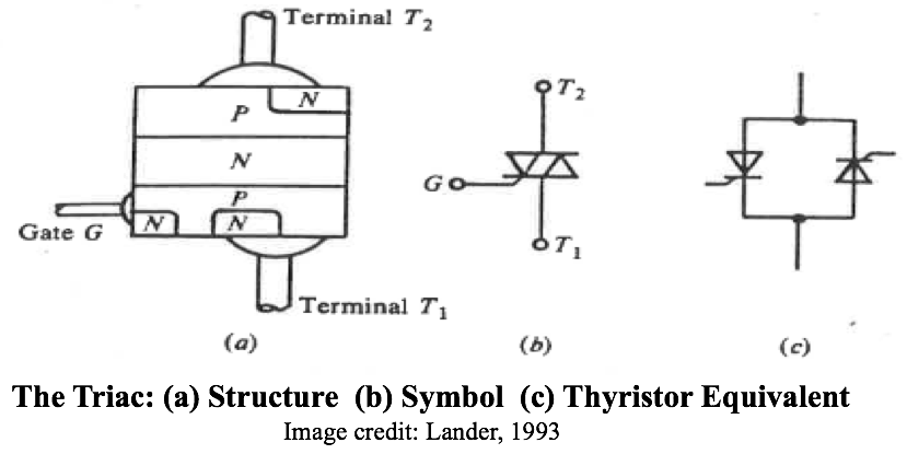
The Triac can be switched ‘on’ by either positive or negative gate current. In practice, negative gate current is always used.
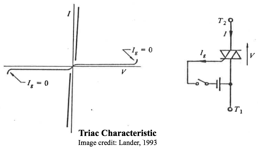
The Triac has a much more limited application than the thyristor mainly in heating and lighting control (e.g. light dimmers).
-
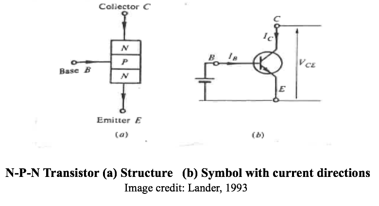
The Power Bipolar Junction Transistor (BJT)
The power transistor is a three-layer N-P-N or P-N-P device as shown
The BJT Characteristics
The following points of interest may be noted.
- In working range IC, is a function of IB. Hence a change in IB gives a amplified change in IC for a given collector-emitter voltage, VCE.
- As, VCE, is increased, the device reaches a breakdown level.
- Reversal of VCE will breakdown the base-emitter junction at a low voltage, around 10 V. For this reason the transistor is not operated in this reverse mode.
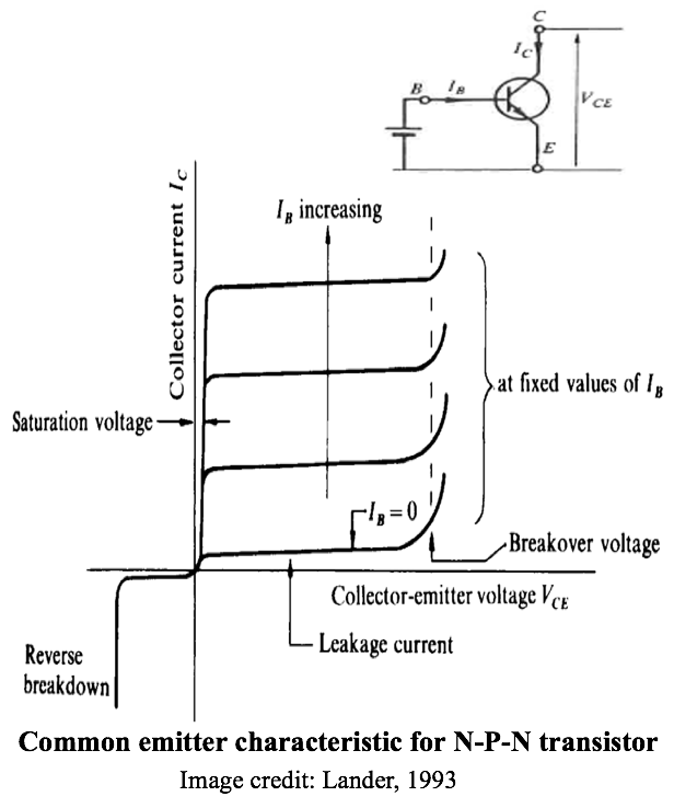
The power loss in the transistor is given by VCE x IC. The loss can be high if the BJT is operated in amplification mode.
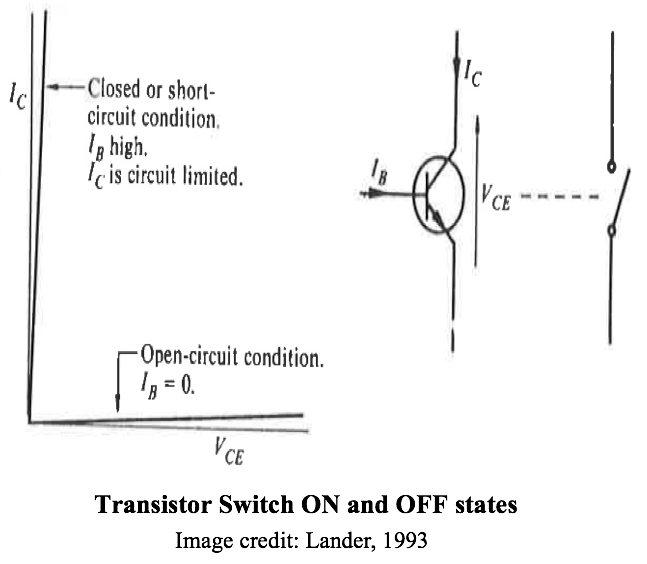
In practice the transistor is operated as a switch for power applications. As a switch the power transistor has two states as shown.
Thus for zero base current the output is effectively an open circuit, whereas with a base current which takes the device into saturation, it is effectively a closed switch.
The BJT Switching
Typical waveforms when the transistor is operated as a switch are shown below.
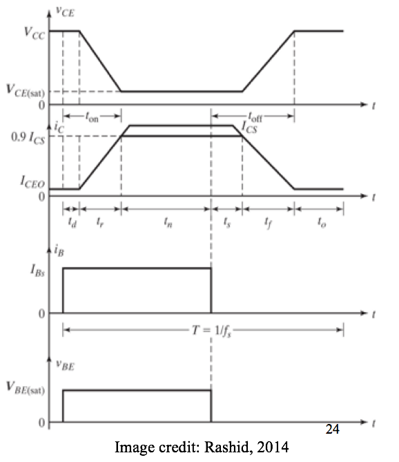
As vB rises from 0 to VBE(sat) and IB rises to IBs, the collector current does not respond immediately due to the internal capacitances. vCE follows i inversely.
When the BJT is fully ON, the power loss is small being due to the product of the small saturation voltage (typically 1.1 V for silicon power transistor) and the large collector current when the transistor is conducting.
The BJT Switching losses
The transistor switching losses, on the other hand, can be high due to high VCE and iC.
The instantaneous voltage, current and power during switch on and switch off are be shown graphically in the figure below.
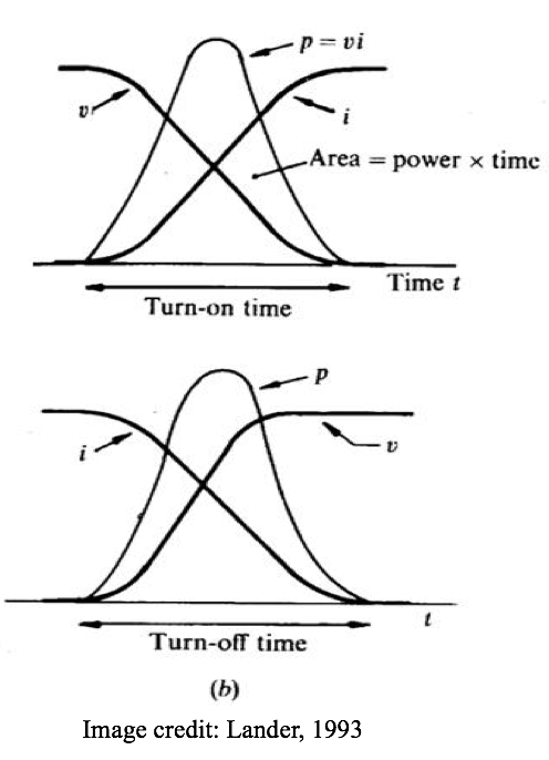
The exact switching loss depends on load as well as the form of the base current change. This means that for a high switching frequency the predominant loss is that due to switching.
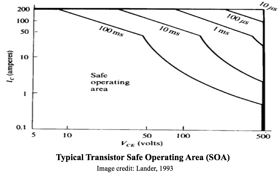
The BJT Safe Operating Area (SOA)
To exploit the power transistor fully without overheating during switching, use can be made of the safe operating area characteristics.
The BJT Power Loss Example
During turn-on and turn-off of a power transistor supplying a resistive load the voltage and current variations are as shown in figure as idealized linear changes with time.
Given that, for each, the switching energy loss is given by (VI/6)T, where V is the off state voltage, I the on-state current and T is the switching time, determine the mean power loss due to switching at a frequency of 10 kHz.
If the transistor is operating with a duty cycle of 0.5, determine the conduction loss if the collector-emitter voltage, vCE is 2.1 V and the current iC is 200 A. Hence, determine the total device loss.
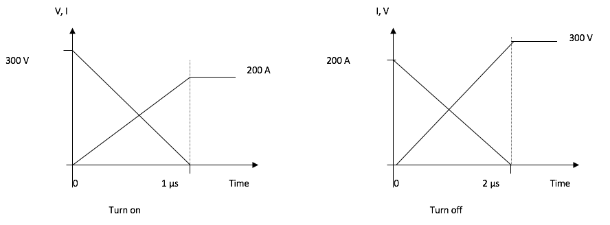
Solution
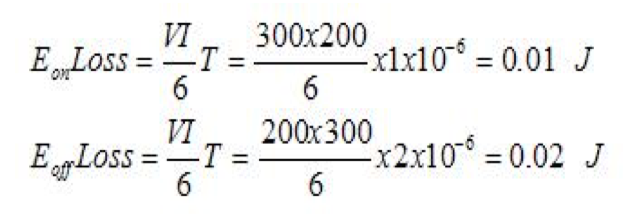
Mean power loss is given by energy loss x switching frequency
Switching loss = (0.01 + 0.02)x10x103
Conduction loss (for duty cycle of 0.5) = 200 A x 2.1 V x 0.5 = 210W
Thus total power loss = Psw + Pcond = 300 + 210 = 510W
-
Power Metal Oxide Semiconductor Field Effect Transistor (MOSFET)
Historically, bipolar semiconductor devices (i.e, diode, transistor, thyristor, triac, GTO etc) have been the front runners in power electronic switches. However all bipolar devices, suffer from disadvantages:
- limited switching speeds;
- large control power requirement which complicates the control circuit design;
- bipolar devices cannot be paralleled easily.
The power MOS field effect transistor (MOSFET) evolved from the MOS integrated circuit technology in 1980. The MOSFET promised extremely low input power levels and no inherent limitation to the switching speed.
Thus, it opened up the possibility of increasing the operating frequency in power electronic systems resulting in reduction in size and weight.
Two types: "n-channel" and "p-channel" devices are made, but the n-channel type are available in higher ratings, so these are used more widely.
MOSFET Characteristics
- Apply gate voltage to switch ON
- Remove gate voltage to switch OFF
- Match demand current with gate voltage
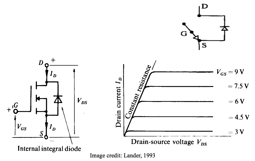
Output Characteristics
For any value of VGS above the threshold level, initially for low values of VDS, the device behaves like a resistance, the current increasing linearly with voltage. The ratio VDS/ID is the total resistance in the ON state, equal to RDS(ON). The magnitude of RDS(ON) determines the forward voltage drop and the internal power dissipation in the device, in its ON state, for a drain current ID. These are given by:
Vf = IDRDS(ON) and Pdis = I2DRDS(ON)
Safe operating area (SOA) of a MOSFET
The SOA of a MOSFET is plotted on a log-log graph. On the top, the SOA is restricted by the absolute maximum value of the drain current (IDM).
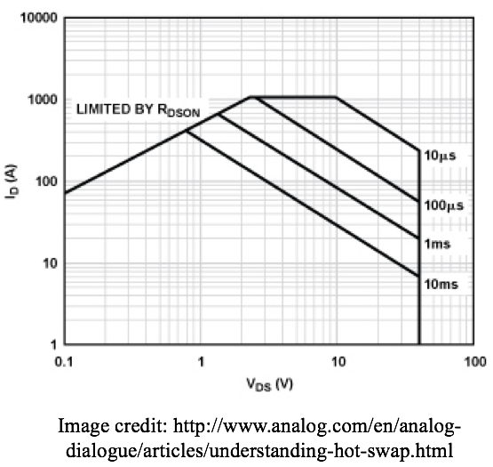
To the left, operating restriction arise due to the non zero value of rDS(ON) corresponding to vGS = vGS(Max).
To the right, the first restriction is due to the limit on the maximum permissible junction temperature rise.
The final operation limit to the extreme right of the SOA arises due to the maximum permissible drain source voltage (VDSS) which is decided by the avalanche break down voltage.
-
Insulated Gate Bipolar Transistors (IGBTs)
IGBT is a power switch that combines advantages of MOSFET and BJT.
IGBT compared with power MOSFETs and power BJTs
Like the power MOSFET,
- It is a voltage controlled switch
- It’s switching control requirements are the same as for a MOSFET.
- The switching speeds of IGBTs are higher than those of BJTs
Like the power BJT:
- Its ON state voltage drop is lower than that of a power MOSFET .
- The IGBT has no integral reverse diode.
- The IGBT has no significant reverse voltaic blocking capability. The maximum reverse voltage is typically well below 10 V.
IGBTs are manufactured in voltage and current ratings extending beyond those available in power MOSFETs - devices with voltage ratings of 1200V and current rating of 600 A are available.
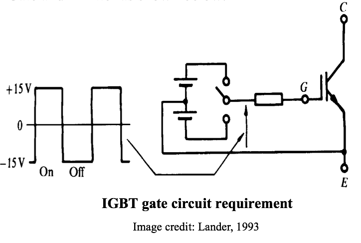
Switch ON and Switch OFF of an IGBT
The IGBT is switched ON by applying a positive voltage between Gate and Emitter. It can be switched OFF by applying a negative voltage between Gate and Emitter as shown below.
Ideal characteristics of Power devices
Ideally, the power devices should have the following properties:
- unlimited voltage and current ratings
- instant turn-on and turn-off times
- zero leakage current
- zero conduction and switching loss
- zero gate or base power requirement
- ability to withstand current overloads and voltage transient
- easy to protect against spurious turn-on and fault conditions
- low cost and ease of assembly
-
Thyristor and Power transistor comparisons
Thyristor advantages:
- Highest ratings of all the power devices available.
- Very robust.
- Low conduction loss.
Thyristor disadvantages:
- Once turned on, it latches.
- Requires complex commutation circuit to switch the device off.
- Slow switching speeds
Thyristors are used in applications where very high voltages and currents are involved and also where AC supply is used as it exploits its natural zero-crossings for commutation.
Transistor advantages:
- Fast switching speeds.
- Easy to turn on and off.
Transistor disadvantages:
- Lower ratings than thyristors.
- Cannot withstand large reverse voltages.
Transistors are used in applications where low to medium voltages and currents are involved. e.g. DC to AC conversion and other DC switching circuits like switch mode power supply, where high switching frequencies are desirable and no need for natural commutation to switch off devices.
-
Check your understanding by answering the following:
Explain, with the aid of a block diagram, what is power electronics.
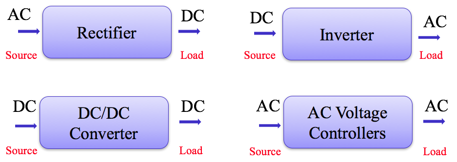
- Name the 4 different families of power electronic converters and their main conversion function.
- With the aid of a simple diagram, explain the voltage-current characteristics of power diodes. Label your diagram clearly and define all terms used.
- Explain what is meant by “forward blocking” mode of operating thyristors highlighting the difference with the “reverse blocking” mode.
- What is the difference between the latching current and the holding current of a thyristor?
- Discuss the circuit conditions needed for a thyristor to be switched on and off.
- What is the main difference between thyristors and GTOs?
- With the aid of simple waveforms, explain the BJT switching process, and the resultant switching losses it generates.
- MOSFET technology opened up the possibility of enhancing performance of its predecessor bipolar devices. Discuss this statement highlighting the advantages introduced by MOSFETs.
- Discuss the advantages of IGBTs as power semiconductor devices highlighting how they combine merits of BJTs and MOSFETs.
- State FOUR properties of ideal power semiconductor devices.
- Give TWO reasons why thyristors still find many applications in power electronic converters although transistors are easier to control and have much faster switching speeds compared to thyristors.