-
-
Losses and Cooling
The sources of loss in power semiconductor devices may be listed:
1. The loss during forward conduction, which is a function of the forward volt-drop and conduction current. This is the major source of loss at mains and lower-frequency operation.
2. The loss associated with the leakage current during the blocking state.
3. The loss occurring in the gate circuit as a result of the energy input from the gating signal. In practice, with pulse firing these losses are negligible.
4. The switching loss, that is, the energy dissipated in the device during turn-on and turn-off which can be significant when switching is occurring at a high frequency.
The power loss generates heat which leads to a temperature rise in the device. The device needs to cooled in order to keep it with the stated limit to avoid destruction of the device.

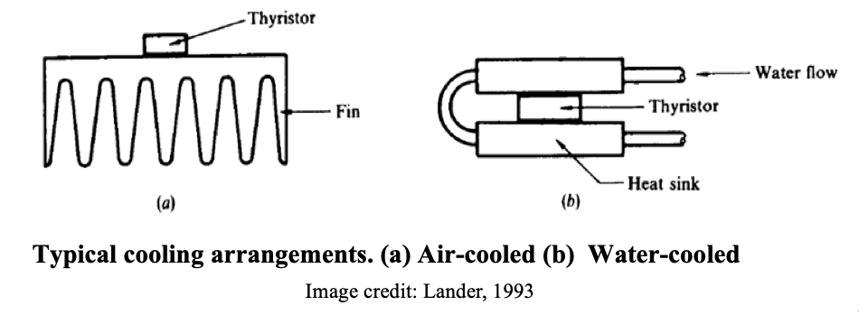
Cooling arrangements
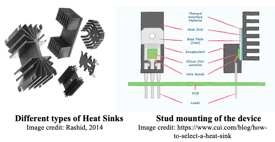
The heat generated in the device is transferred to the base, and then to a heat sink. Heat transfer takes place by convection, to air in the case of the metal-finned heat sink illustrated in (a).
Where the size of the fins is prohibitive, or the level of heat dissipation is very high, the heat sink can be cooled by a water-cooled assembly, as illustrated in (b).
-
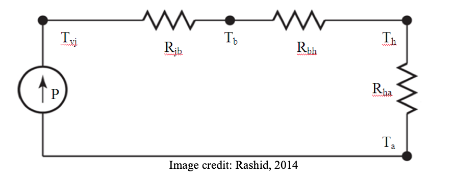
Equivalent circuit of the heat transfer

The heat transfer, P (power loss to be dissipated), is proportional to the temperature difference, the ratio being known as the thermal resistance R:

where Tl and T2 are the temperatures of the hot and cold bodies respectively. Unit of power is the watt, temperature is in oC, and the thermal resistance in oC/W.
The heat flow is from the junction to the base, to the heat sink, to the surroundings, and the total thermal resistance will be the series addition of the individual thermal resistances of each section. The total thermal resistance from the junction to the surroundings (ambient) , Rja is:
Rja =Rjb + Rbh + Rha
where Rjb, Rbh and Rha are the thermal resistances from junction to base, base to heat sink, and heat sink to ambient.
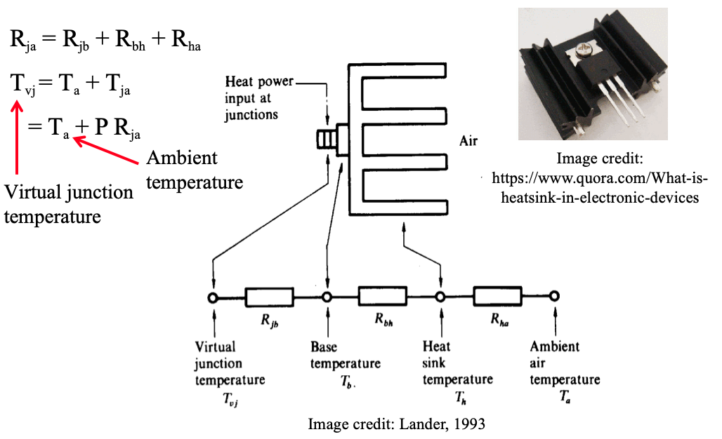
Thus the electrical analog circuit of the heat transfer is as below.
The above calculations all refer to steady-state continuous-current conditions, when the loss is constant, the temperature having settled to a steady value.
-
Choosing a Heat Sink
Wide variety of aluminium heat sinks are commercially available and they use cooling fins to increase the heat transfer capability. The thermal resistance characteristics of a typical heat sink with natural and forced cooling are shown.
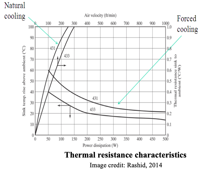
The figure shows the power dissipation against the sink temperature rise for natural cooling.
In forced cooling, the thermal resistance decreases with the air velocity. However, above a certain velocity, the reduction in thermal resistance is not significant. -
Air Coolers
- Conduction, radiation and convection
- Lower thermal resistance by increasing surface area
- Natural Cooling
● Sheet metal (1°C/W)
● Castings/Extruded (0.25 °C/W)- Thermal resistance non linear
- Temperature, environment (reflections)- Forced cooling lowers thermal resistance to 20% of natural cooling
Liquid Cooling
- Hollow liquid-carrying bus-bars
- Electrical insulated couplings
- Compact assembly
- Totally enclosed
- Typically 0.025°C/W for water at 0.07 Litre/sec
-
Mounting Devices on to Heat Sinks
The contact area between the device and heat sink is extremely important to minimize the thermal resistance between the case and sink. The surfaces should be flat, smooth and free of dirt, corrosion, and surface oxides. Silicone greases are normally applied to improve the heat transfer capability. The proper installation procedures are usually recommended by the device manufacturers.
-
Transient thermal response
The thermal impedance of a power device is very small and as a result the junction temperature of the device varies with the instantaneous power loss. The instantaneous junction temperature must always be maintained lower than the acceptable value. A plot of the transient thermal impedance versus time is supplied by the device manufacturers as a part of data sheet:
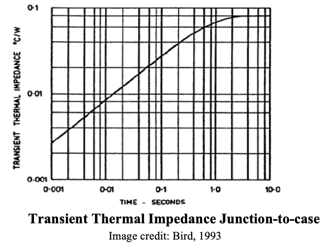
Using the transient thermal impedance and a plot of power loss against time can be used to calculate the temperature variations with time.
Knowledge of excessive temperature rise of the heat sinks are used to switch off the power converters, especially in high power applications
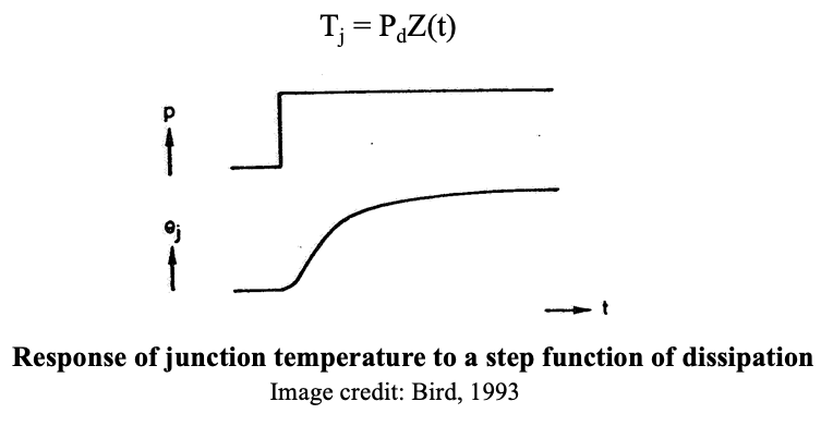
The instantaneous junction temperature rise
The transient thermal impedance using step response of a first order system. If Z0 is the steady-state junction case thermal impedance, the instantaneous thermal impedance can be expressed as:
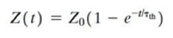
where τth is the thermal time constant of the device. If the power loss is Pd, the instantaneous junction temperature rise above the case is:
-
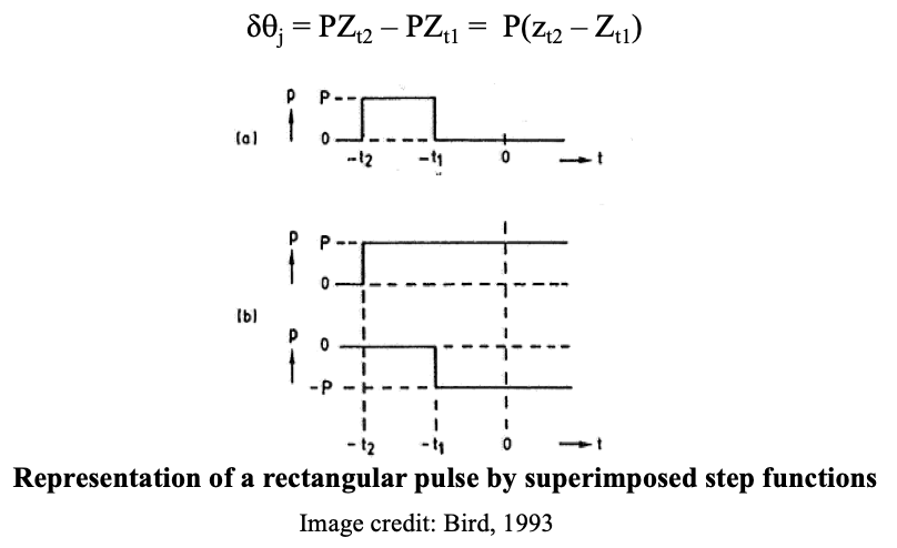
Single rectangular power pulse
The pulse is represented as the sum of two step functions, +P occurring at t2 and -P at t1 as in (b).
The junction temperature rise at t = 0 is then the sum of the separate effects of the two step functions:
Example
Estimate the instantaneous junction temperature rise at t = 0 due to a rectangular current pulse (similar to the figure above) of 1000 A of 10 ms duration, followed by an interval (-t1) of 10 ms at zero current. The voltage drop across the thyristor at 1000 A is 2.2 V.
Use the Transient Thermal Impedance Junction-to-case curve on slide 12 to read of the thermal impedances.
Solution
Current is 1000 A; Voltage drop at thyristor is 2.2 V. The pulse is 10 ms duration, followed by an interval (-t1) of 10 ms at zero as shown below: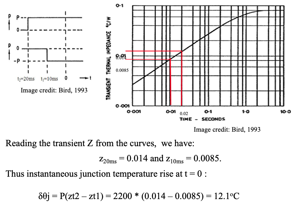
-
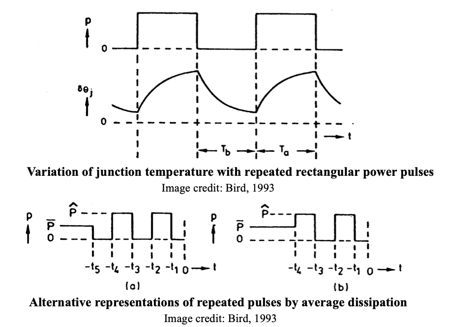
Repeated rectangular power pulses
Example
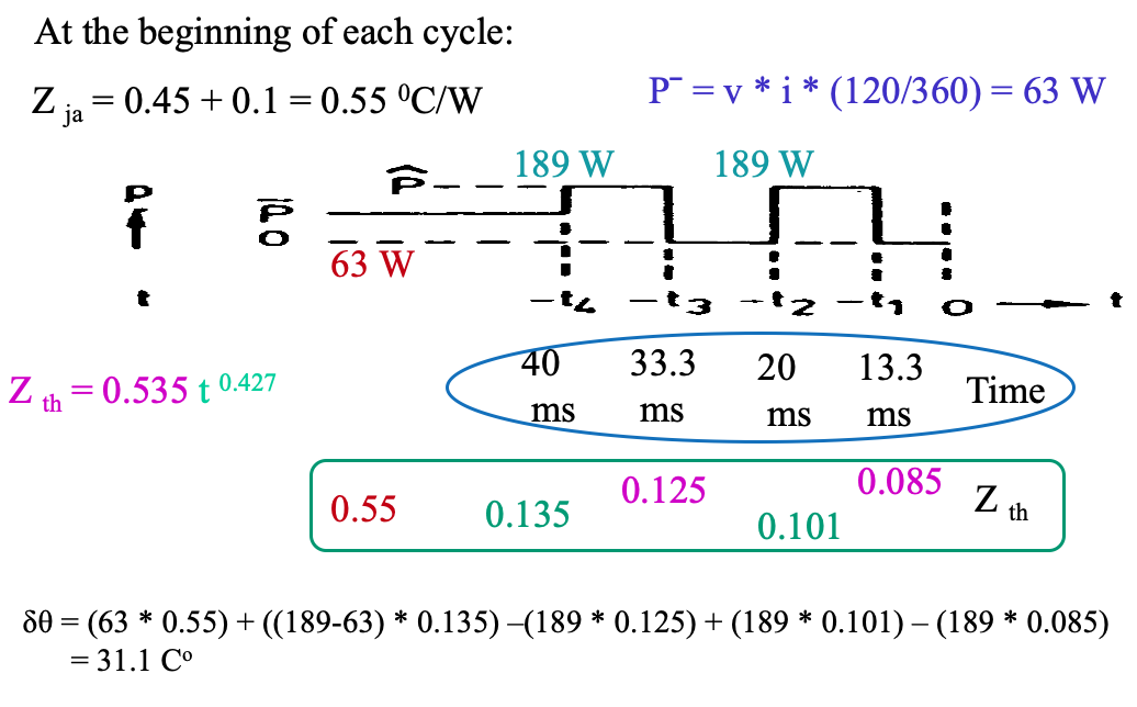
A fully-controlled three-phase bridge converter supplies a current of 100 A d.c. (assumed smooth). The thyristor voltage drop at 100 A is 1.89 V, the junction-to-base thermal resistance is 0.45 Co/W and the mounting thermal resistance is 0.1 oC/W.
The transient thermal impedance can be represented with sufficient accuracy over the, range in question by the empirical relationship Zth(t) = 0.535 t 0.427 C o/W (t in seconds), or at 50 Hz, Zth(t) = 0.00815(wto) 0.427C o /W.
Estimate the junction-to-cooler temperature rise at the beginning of each 120o conduction period at 50 Hz.
Solution
-
Devices’ protection
- Thermal runaway
- Heat sinks and cooling systems- High dv/dt and di/dt
- Snubber circuit- High dv/dt and di/dt
- Snubber circuit- Reverse recovery transients
- Snubber and Other fast devices- Supply/load-side transients
- Transient suppressors- Fault conditions
- Fuses and current limiting devices
- Thermal runaway
-
Check your understanding by answering the following:
- Discuss THREE sources of losses in power semiconductor devices.
- Discuss different cooling arrangements used in thermal management of power switching devices highlighting the main properties of each when choosing a heat sink.
- Draw the electrical equivalent circuit for the thermal process of cooling power semiconductor devices using heatsinks. Explain the meaning of each parameters used in the circuit.
- Discuss TWO mounting factors that minimize the thermal resistance between the case of a power semiconductor device and a heat sink.
- Explain why snubber circuits are used in conjunction with power semiconductor devices.