-
-
Conduction overlap in rectifier circuits
In previous lectures, the assumption was made that the transfer or commutation of the current from one diode (or thyristor) to the next took place instantaneously. In practice, inductance and resistance is always present in the supply source, and time is required for a current to change from one device to the other. The net result is that the current communication is delayed, as it takes a finite time for the current to decay to zero in the outgoing diode (or thyristor), while the current will rise at the same rate in the incoming diode (or thyristor). To explain the phenomenon associated with the current transfer, the three phase uncontrolled half-wave rectifier connection can be used.
Overlap in uncontrolled 3-ph half-wave rectifier
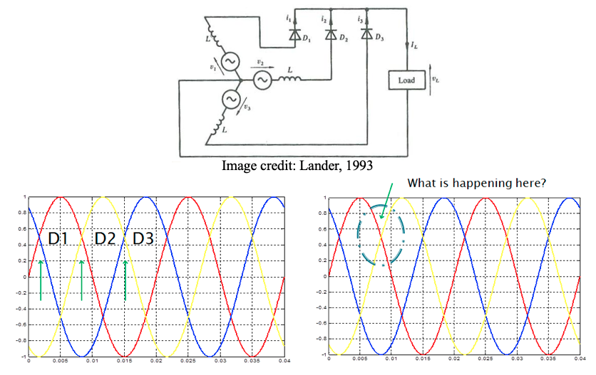
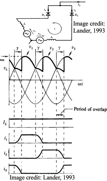
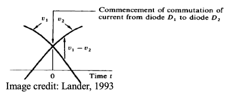
At commutation there is an angular period γ during which both the outgoing diode and incoming diode are conducting. This is known as the overlap period, and γ is defined as the commutation angle or the angle of overlap.
During the overlap period, the load current is the addition of the two diode currents. The load voltage is the mean of the two conducting phases, the effect of overlap being to reduce the mean level.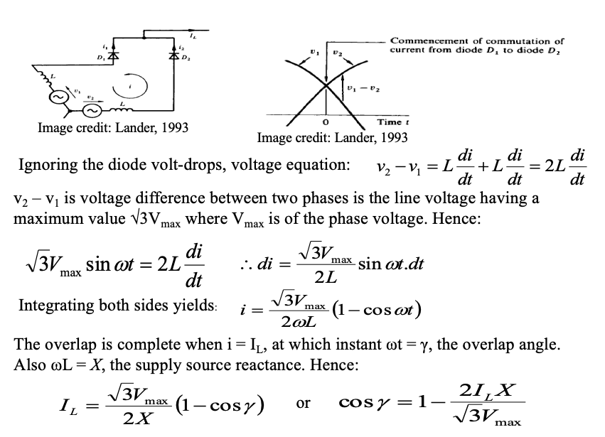
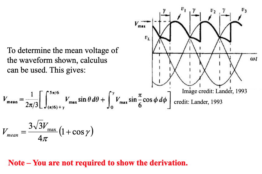
Overlap in controlled rectifiers
In controlled rectifiers, the overlap will lead to the waveform shown, where it can be seen that with a firing delay angle α, a finite voltage is present from the start of commutation.
-
Regulation in rectifier circuits
In the case of the rectifier, regulation describes the drop in mean voltage with load relative to the no-load or open-circuit condition.
There are three main sources contributing to loss of output voltage:
1. The voltage drop across the diodes and/or thyristors.
2. The resistance of the a.c. supply source and conductors.
3. The a.c. supply source inductance.
These three voltage drops can be represented respectively by the three resistors R1, R2 and R3 in the equivalent circuit. The open-circuit voltage is given by V0 and the actual load voltage by VL. If the load current IL is taken to be level, that is, a pure direct current, then any voltage drop can only be represented by resistors.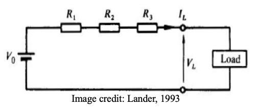
The voltage drop across the thyristors and diodes (represented by R1) is given by a constant volt-drop (junction potential) plus a resistance for the bulk of the silicon.
The resistance of the leads and a.c. source resistance (represented by R2) can be considered constant in most cases.
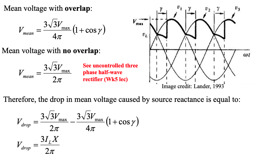
The voltage drop due to the a.c. supply source inductance is the overlap effect, and was calculated for the three-phase half-wave uncontrolled rectifier (3X/2π)IL.
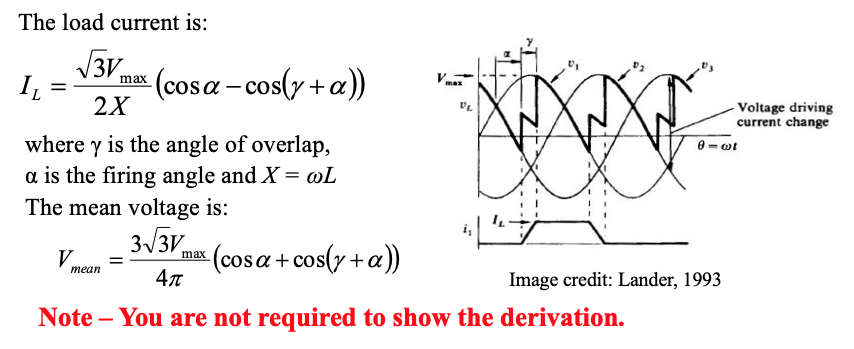
For the Fully controlled three phase rectifier this works out to be: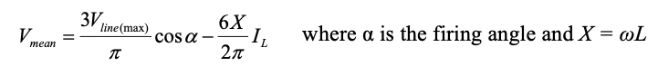
Examination of this equation shows that the load voltage is reduced by (6X/2π)IL for the six-pulse output (notice the double voltage drop compared to half-wave); and is represented in the equivalent circuit as a resistance of value (6X/2π).
Generalized equation for p-pulse rectifiers
A general expression for the mean load voltage of a p-pulse fully-controlled rectifier, including the effects of the overlap angle γ, can be derived by using the preceding analysis. These are stated here:
-
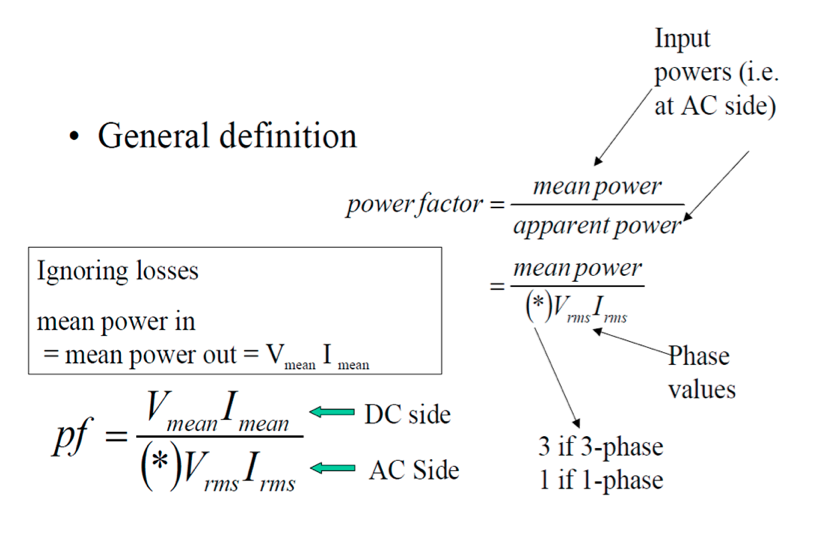
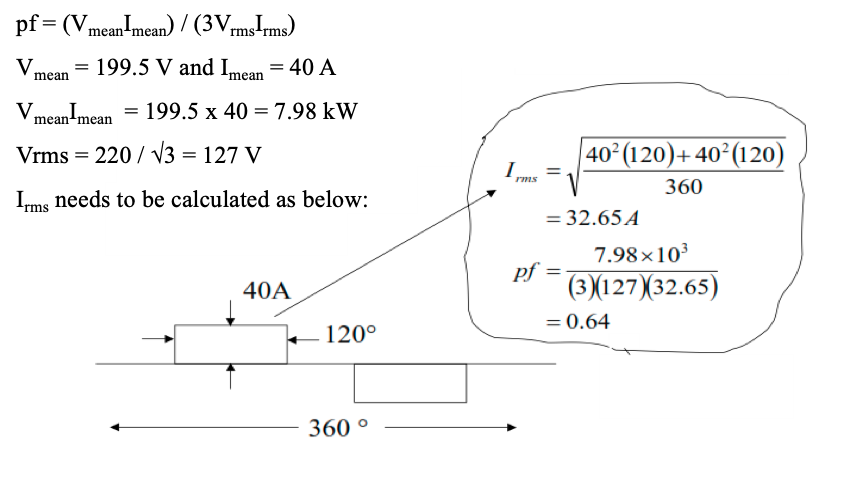
Input Power factor
Worked example on regulation and power factor
Fully-controlled three-phase bridge converter is supplied at 220V from a 50-Hz AC supply with a source reactance of 0.24 Ohms per phase and which delivers a continuous current of 40A to a load.
a) Determine the mean output voltage of the converter for a phase delay angle of 45° (assume device drop of 0.7V)
b) Determine the input power factor for the above firing delay angle.Solution
a)
The equivalent circuit for this converter is shown below. Note: as this is bridge converter, the device voltage drop will be 2 x 0.7 = 1.4 V.
Drop due to overlap is pX/2π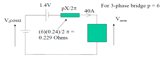
Total voltage drop in the circuit = 1.4 + 40 x 0.229 = 10.57 V
Vo = (pVmax/π) x sin(π/p) = (6 x √2 x 220/π) x sin(π/6) = 297.1 V
V0cosα = (297.1) x cos 45o = 210.1 V
Thus Vmean = 210.1 – 10.57 = 199.5 V
b)
-
Check your understanding by answering the following:
Discuss the impact that source inductance has on commutation in rectifier circuits and the effect on mean output voltage
OR IN OTHER WORDS
What is the main cause for current commutation delay in rectifier circuits? Explain your answer inState THREE main sources contributing to loss of output voltage in rectifier circuits.
- Insert Content Here 6
- Insert Content Here 7