02
-
Printed Circuit Board (PCB) Design
- Aim
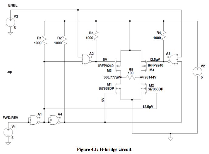
The aim is to design a PCB for an H-bridge motor control circuit. The circuit diagram is shown in section 6.1 and the suggested H-bridge PCB layout in section 6.2.
Circuit Simulation Procedure Using LTspice
You will use LTspice (www.linear.com/designtools/software/#LTspice) for circuit simulation (it is provided free by Linear Technology). To become familiar with LTspice, watch the LTspiceIV Overview video.
Start a new schematic and capture the H-bridge circuit as shown in Figure 4.1. Note that the motor has been replaced with a resistor (R5) for simulation purposes.
Get the logic gates from LTspice's digital library (choose "and"). Once the gates are placed on the schematic, right click on each one and set the value of the attributes as follows:
Value2 => Vhigh = 5 Vlow = 0 Ref = 1.5 SpiceLine => Trise = 5n Tfall = 5n Td = 5n
Regarding the MOSFETs use "nmos" (for M1 & M2) and "pmos" (for M3 & M4). Once these parts are placed on the schematic, right click on them and click on "pick new MOSFET", and select the actual part numbers shown in the schematic above. For the voltage sources V1, V2 and V3 use the part "voltage" and change their value by right clicking on the "V".
To run a DC operating point analysis click on the "running man" icon and select the last tab ("DC op pnt"), then click OK. Assuming the simulation ran without errors, close the text pop- up and place several data labels to view the voltage on selected points in the circuit. To do this, right click on an empty part of the schematic and select View > Place .op Data Label. You can see how the circuit works by changing the voltages applied to the ENABLE and FWD/REV inputs and running the simulation again. The voltages shown on the data labels should change accordingly.
- LTSpice Demonstration Video 📹
- LT Spice Software - Video Demonstration
- Please stop the video before closing the lightbox
- Aim
-
PCB Design Using EAGLE
- You will use the PCB design program EAGLE (www.cadsoftusa.com/download-eagle) which can be run as freeware (with some limitations). There are tutorials, videos and manuals available on the EAGLE web site (www.cadsoftusa.com/training). Below is a procedure using typed commands to control EAGLE. You type the commands in the bar directly above the drawing area. Alternatively, the GUI menu and icons can also be used.
You first click on the icon and then on the object on the schematic. Do not select the object first and then click on the icon.
To create a new directory
• Click on Options > Directories > Projects > Browse > Make New Folder
Starting a new project
Schematic capture procedure
• Make sure that all component libraries are available by the following procedure: from the schematic page select Library > Use and with the shift button select all the libraries.
• Cmd > ADD 74LS01N (expand 74xx-eu > 74*01 and select the 74LS part; then place NAND gates A, B, C & D)
• Cmd > ADD PMOSFET_NTO220BV (place two MOSFETs Q1, Q2)
• Cmd > ADD PMOSFET_PTO220BV (place two MOSFETs Q3, Q4)
• Cmd > ADD R-EU* (select from parts library resistors 0207/12 and place four resistors R1, R2, R3, R4)
• Cmd > ADD C-EU* (select from parts menu capacitor C025-030X050 (place capacitor C1)
• Right click on NAND gate A , select INVOKE , select gate P and OK (NAND pwr pins visible)
• Cmd > ADD WIREPAD* (select from parts library WIREPAD 2,54/1,0 and place 6 WIREPADS connections and rename them as 0V, +5V, fwd/rev, enable, M+, M-)
• Cmd > NET (proceed to connect the schematic as shown in the schematic diagram layout, before doing this clear the main drawing area by moving the components to the periphery of the board)
- Eagle Schematic Design - Demonstration Video 📹
- PCB layout procedure
- From the schematic layout click the icon on the top toolbar that switches to the Board Layout page (or select File > Switch to board from the menu). This will show the Board Layout screen, notice that all components are place to the left of the board.
- FCmd > CLASS (change width to 20 mil)
- Cmd > WIRE (select layer 20 Dimension from the top toolbar menu; use this layer to draw the Board Outline; starting from the origin - a cross symbol - draw a square board of 2.5 x 2.5 inches)
- Get familiar with the toolbar menu on the left side of the page. Use these icons to position the components into the positions as shown in the PCB layout diagram in Figure 6.2.
- To AUTOROUTE circuit board as a single sided bottom copper layer do the following:
* - Cmd > RECT (select layer 41 tRestrict from the top toolbar menu; click on the board origin drag the rectangle to the top right corner of the board; this fixes the keep-out area of the autorouter)
* - Cmd > AUTO (select OK; the autorouter will attempt to use the NETS to find a path for the copper layer connections; any routes that cannot be found by the autorouter will be left for manual routing)
- To MANUAL route:
- Cmd > WIRE (select the Bottom layer from the top toolbar - layer 16 Bottom -; the colour of the bottom copper layer is blue and the colour of the top copper layer - layer 1 Top - is red; now manually connect the remaining copper tracks without crossing over tracks of the same layer colour; any red layer tracks will represent a wire link on the top of the circuit board)
- Helpful tips:
* - Cmd > Ripup (will remove a track)
* - Cmd > Ratsnest (will show remaining un-routed tracks)
* - Cmd > Ripup (and click on traffic lights icon to remove all tracks)
* - Cmd > Class (change default width to 16 mil this will ensure that the autorouter will use a minimum track width of 16 mil)
* - Cmd > Show (and left click on the component pad in the PCB layout to show all the connections to that pad)
- To generate the artwork (Gerber files):
* Click on the CAM processor icon (next to the printer icon)
* - On the CAM processor dialog box menu select File > Open > Job
* - Select gerb274x.cam and click on the Open button.
* - Click on Process Job and the Gerber files will be created in your project folder.
- To generate the artwork (Gerber files):
You can check the Gerber files using the free Gerber viewer GC-PREVUE (www.graphicode.com). To view the files use File > Import (not File > Open).
- Eagle PCB Design - Demonstration Video 📹
- Eagle Schematic Design - Demonstration Video
- Please stop the video before closing the lightbox
- Eagle PCB Design - Demonstration Video
- Please stop the video before closing the lightbox
- You will use the PCB design program EAGLE (www.cadsoftusa.com/download-eagle) which can be run as freeware (with some limitations). There are tutorials, videos and manuals available on the EAGLE web site (www.cadsoftusa.com/training). Below is a procedure using typed commands to control EAGLE. You type the commands in the bar directly above the drawing area. Alternatively, the GUI menu and icons can also be used.
-
- Multisim H Bridge Exercise - Video Demonstration
- Please stop the video before closing the lightbox