Wk 9 & 10

Power in AC Circuits
- Introduction
- Two-port Networks
- The Decibel (dB)
- Frequency Response
- A High-Pass $RC$ Network
- A Low-Pass $RC$ Network
- A Low-Pass $RL$ Network
- A High-Pass $RL$ Network
- A Comparison of $RC$ and $RL$ Networks
- Bode Diagrams
- Combining the Effects of Several Stages
- $RLC$ Circuits and Resonance
- Filters
- Stray Capacitance and Inductance
Introduction
- Having now looked at the AC behaviour of simple components, we can consider their effects on the frequency characteristics of simple circuits
- While the properties of a pure resistance are not affected by the frequency of the signal concerned, this is not true of reactive components
- We will start with a few basic concepts and then look at the characteristics of simple combinations of resistors, capacitors and inductors
-
(Continued)
- Sample gains expressed in dBs
- Using dBs simplifies calculation in cascaded circuits
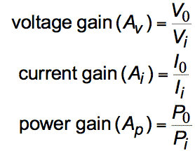
- Power gain is related to voltage gain

- If $R _1 = R_2$
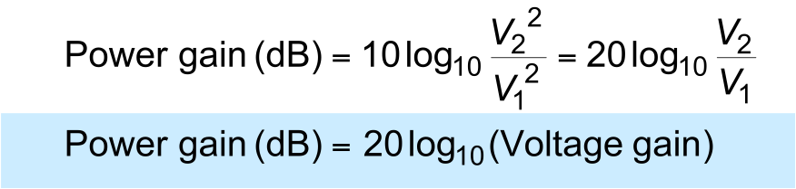
- This expression is often used even when $R_1 \mathrel{{=}\llap{/}} R _2$
– see Example 8.4 in the course text
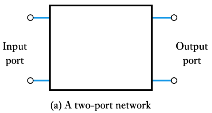
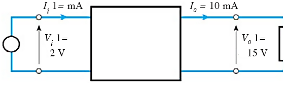
Two-port Networks
- A two-port network has two ports:
– an input port
– an output port
- We then define voltages and currents at the input and output
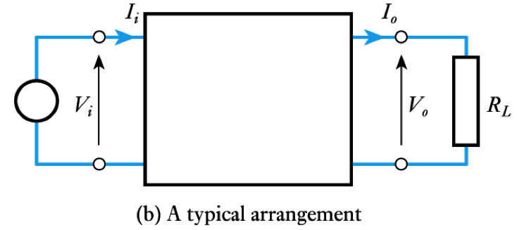
- Then
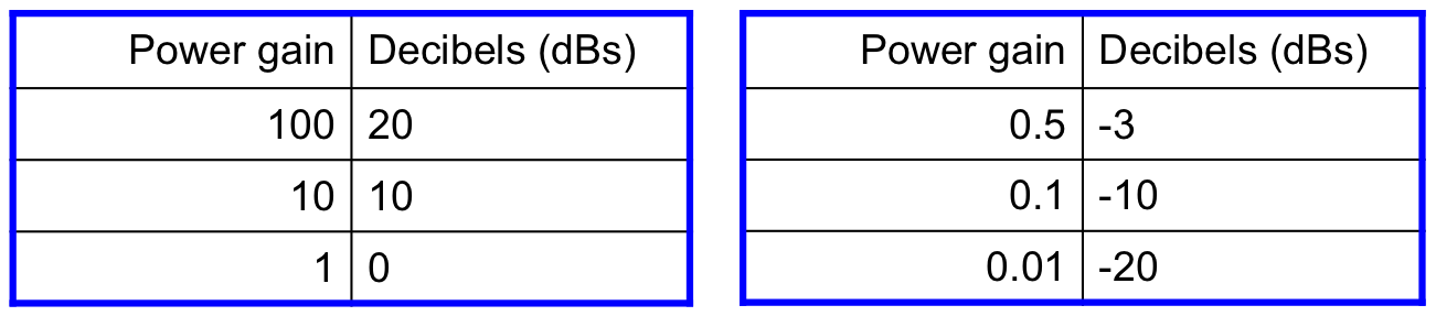
The Decibel (dB)
- The power gain of modern electronic amplifiers is often very high, gains of $10^6$ or $10^7$ being common
- With such large numbers it is often convenient to use a logarithmic expression for gain
- This is often done using decibels
- The decibel is a dimensionless figure for power gain
\begin{align*} \large \text{Power gain (dB)} = 10 \text{ log}_{10} \frac{P_2}{P_1} \end{align*}
- Sample gains expressed in dBs
-
(Continued)
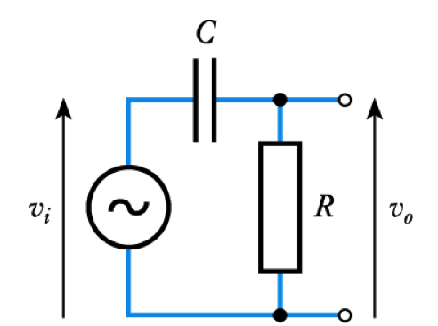
- Clearly the transfer function is

- 📷 See as circuit diagram
- At high frequencies
– $\omega$ is large, voltage gain ≈ $1$
- At low frequencies
– $\omega$ is small, voltage gain → $0$
- Since the denominator has real and imaginary parts, the magnitude of the voltage gain is $$ \text{|Voltage gain |} = \frac{1}{\sqrt{1^2 + \bigg(\frac{1}{\omega CR}\bigg) ^2} } $$
- 📷 See as circuit diagram
- When $1 / \omega \;CR = 1$
$$\text{|Voltage gain |} = \frac{1}{\sqrt{1+1}} = \frac{1}{\sqrt{2}} = 0.707$$- This is a halving of power, or a fall in gain of $3$ dB
- The half power point is the cut-off frequency of the circuit
– the angular frequency $\omega _C$ at which this occurs is given by
\begin{align*} \frac{1}{\omega _C CR}=& 1 \\ \\ \omega _C = \frac{1}{CR}=& \frac{1}{ \text{T}} \text{rad/s} \end{align*}
– where Τ is the time constant of the $CR$ network. Also
$$ f_C = \frac{\omega_C}{2 \pi} = \frac{1}{2 \pi CR} \text{Hz} $$
Frequency response
- Since the characteristics of reactive components change with frequency, the behaviour of circuits using these components will also change
- The way in which the gain of a circuit changes with frequency is termed its frequency response
- These variations take the form of variations in the magnitude of the gain and in the phase response
- We will start by considering very simple circuits
- Consider the potential divider shown here
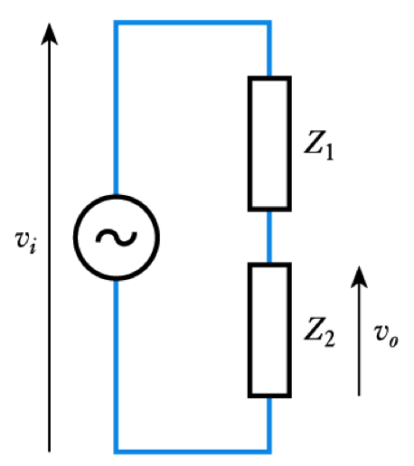
– from our earlier consideration of the circuit
$$ \large {V_o = V_i \times \frac{Z_2}{Z_1 + Z_2}}$$
– rearranging, the gain of the circuit is
$$\large {\frac{V_o}{V_i} = \frac{Z_2}{Z_1 + Z_2}}$$
– this is also called the transfer function of the circuit
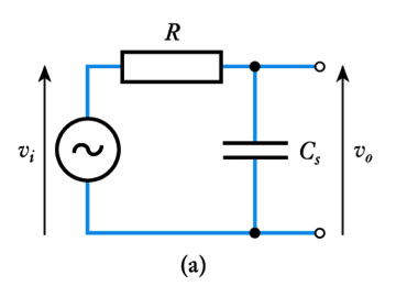
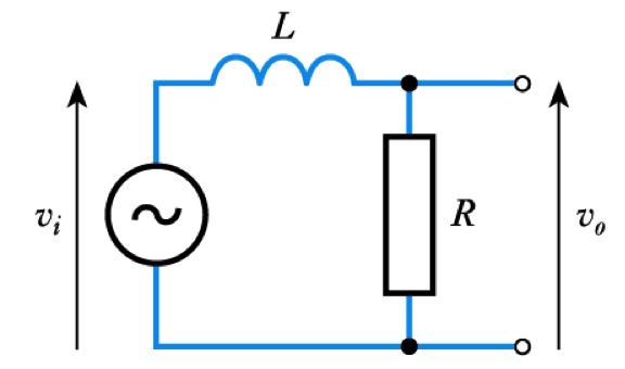
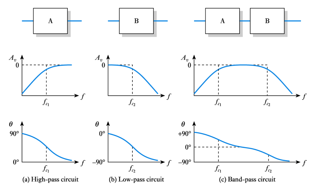
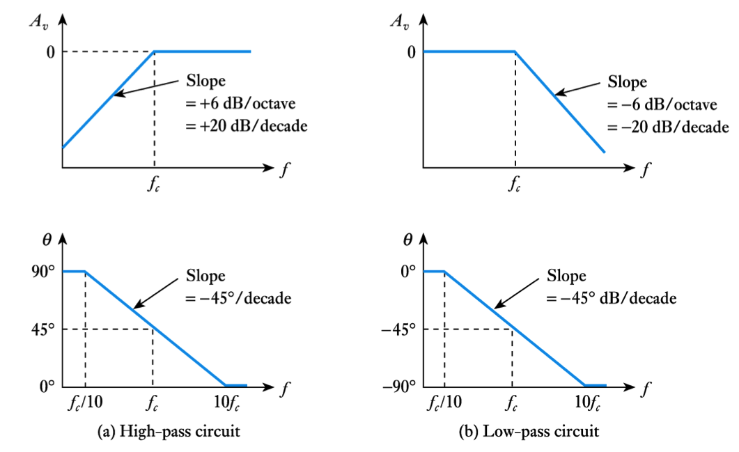
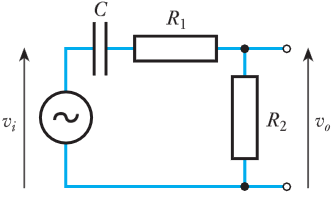
A High-Pass RC Network
- Consider the following circuit
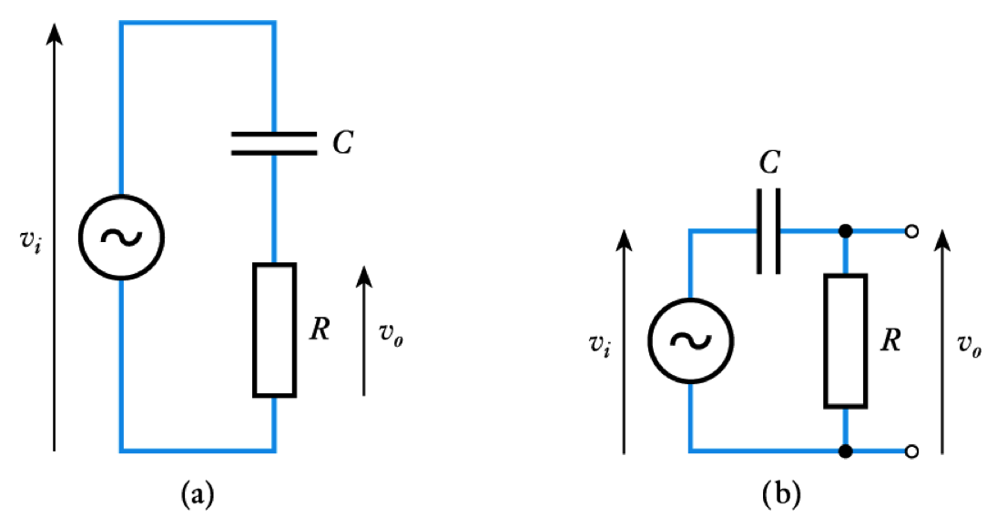
- Clearly the transfer function is
-
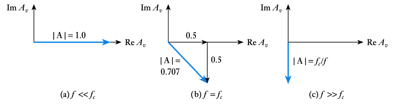
- The behaviour in these three regions can be illustrated using phasor diagrams
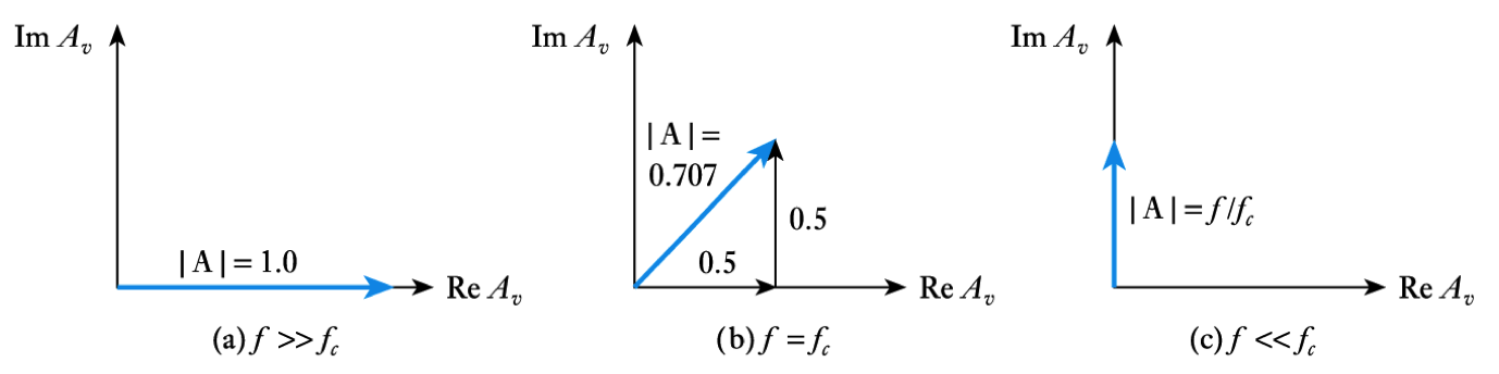
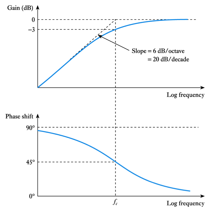
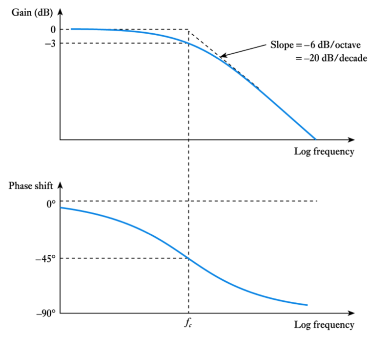
- At low frequencies the gain is linearly related to frequency. It falls at -6dB/octave (-20dB/decade)
- Frequency response of the high-pass network
– the gain response has two asymptotes that meet at the cut-off frequency– figures of this form are called Bode diagrams
(Continued)
- Substituting $\omega = 2 \; \pi \; f $ and $CR = 1/2 \; \pi \; f_C$ in the earlier equation gives

- This is the general form of the gain of the circuit
- It is clear that both the magnitude of the gain and the phase angle vary with frequency
- Consider the behaviour of the circuit at different frequencies:
- When $f$ > > $f_c$
– $ f _c / f $ < < $1$, the voltage gain ≈ $1$
- When $f = f_c$

- When $f$ < < $f_c$
\begin{align*} \frac{V_o}{V_i} = \frac{1}{1-j \frac{\large f_c}{f}} \text{≈} \frac{1}{- j \frac{\large f_c}{f}} = j \frac{f}{\large f_c} \end{align*} - The behaviour in these three regions can be illustrated using phasor diagrams
-
- Therefore
– the angular frequency $\omega _C$ at which this occurs is given by
\begin{align*} \omega _C CR =& 1 \\ \\ \omega _C = \frac{1}{CR} =& \frac{1}{\text{T}} \text{rad/s} \end{align*}
– where Τ is the time constant of the $CR$ network, and as before
$$ f _C = \frac{\omega _C}{2 \pi} = \frac{1}{2 \pi CR} \text{Hz} $$
- Substituting $\omega = 2 \; \pi \; f \text{ and } CR = 1/2 \; \pi \; f_C$ in the earlier equation gives

- This is similar, but not the same, as the transfer function for the high-pass network
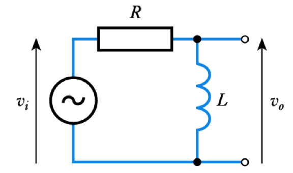
A Low-Pass RC Network
- Transposing the C and R gives
 \begin{align*} \frac{V_o}{V_i} = \frac{Z_C}{Z_R + Z_C}= \frac{-j \frac{\large 1}{\large \omega C}}{R-j \frac{\large 1}{\large \omega C}} = \frac{1}{1+j \omega CR} \end{align*}
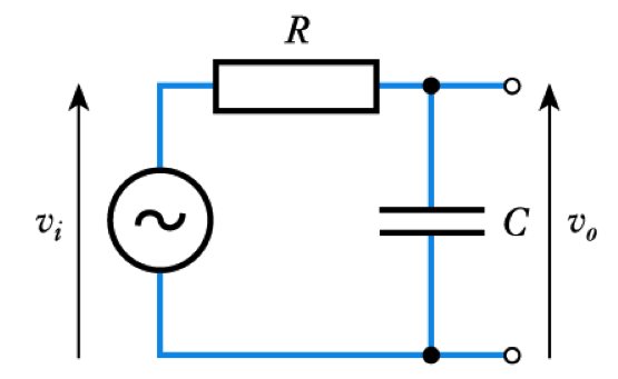
- At high frequencies
– ω is large, voltage gain → 0
- At low frequencies
– ω is small, voltage gain ≈ 1
- A similar analysis to before gives (see reference diagram above)
$$ \text{|Voltage gain |} = \frac{1}{\sqrt{1 + \omega CR ^2} } $$- Therefore when, when ω $CR$ = 1
$$ \text{|Voltage gain |} = \frac{1}{\sqrt{1 + 1}} = \frac{1}{\sqrt{2}} = 0.707 $$- Which is the cut-off frequency
- Therefore
-
- At high frequencies the gain is linearly related to frequency. It falls at 6dB/octave (20dB/decade)
- Frequency response of the low-pass network
– the gain response has two asymptotes that meet at the cut-off frequency
– you might like to compare this with the Bode Diagram for a high-pass network
(Continued)
- Consider the behaviour of this circuit at different frequencies:
- When $f$ < < $f_c$
– $f / f_c $ < < $1$, the voltage gain ≈ $1$
- When $f = f_c$

- When $f$ > > $f_c$

- The behaviour in these three regions can again be illustrated using phasor diagrams
-
A Comparison of RC and RL Networks
- Circuits using $RC$ and $RL$ techniques have similar characteristics
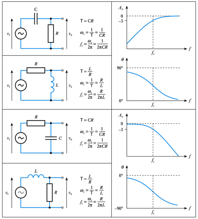
– see Figure 8.12 in the course text
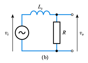
A Low-Pass RL Network
- Low-pass networks can also be produced using $RL$ circuits
– these behave similarly to the corresponding CR circuitA High-Pass RL Network
- High-pass networks can also be produced using $RL$ circuits
– these behave similarly to the corresponding CR circuit
- Circuits using $RC$ and $RL$ techniques have similar characteristics
-
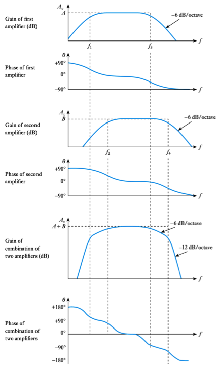
Combining the Effects of Several Stages
- 📷 The effects of several stages ‘add’ in bode diagrams - see here
- Multiple high- and low-pass elements may also be combined
– this is illustrated in Figure 8.16 in the course text
Bode Diagrams
- 🎥 Watch a video on Bode diagrams - Adobe Flash video
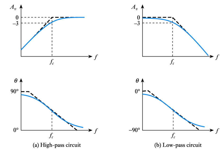
- Straight-line approximations
- Creating more detailed Bode diagrams
- 📷 The effects of several stages ‘add’ in bode diagrams - see here
-
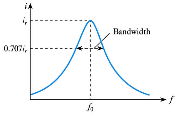
- The series $RLC$ circuit is an acceptor circuit
– the narrowness of bandwidth is determined by the $Q$
\begin{align*} \text{Quality factor } Q = \frac{\small \text{Resonant frequency}}{Bandwidth} = \frac{f_o}{B} \end{align*}
– combining this equation with the earlier one gives
\begin{align*} B = \frac{R}{2 \pi L} \text{Hz} \end{align*}
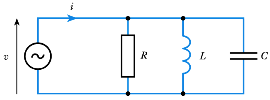
- Parallel $RLC$ circuits
– as before
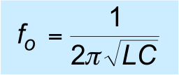
$$ \omega _o = \frac{1}{\sqrt{LC}} \qquad f _o = \frac{1}{2 \pi \sqrt{LC}} $$
- The parallel arrangement is a rejector circuit
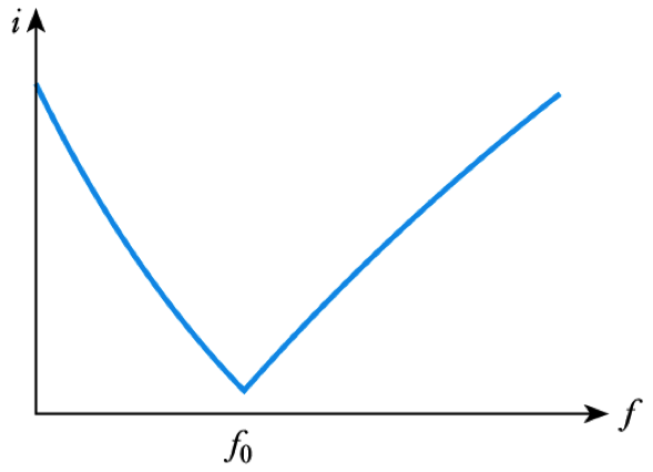
– in the parallel resonant circuit , the impedance is at a maximum at resonance
– the current is at a minimum at resonance– in this circuit
$$ Q = R \sqrt{\bigg(\frac{C}{L}\bigg)} \qquad B = \frac{1}{2 \pi RC} \text{Hz} $$
RLC Circuits and Resonance
- Series $RLC$ circuits
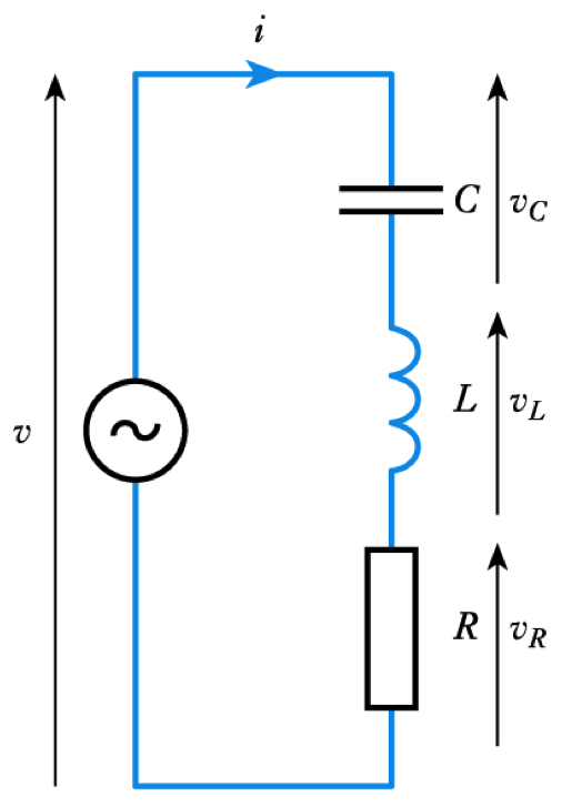
– the impedance is given by
 \begin{align*} Z = R + j \omega L + \frac{1}{j \omega C} = R + j (\omega L -\frac{1}{\omega C }) \end{align*}– if the magnitude of the reactance of the inductor and capacitor are equal, the imaginary part is zero, and the impedance is simply $R$
- This situation is referred to as resonance
– the frequency at which is occurs is the resonant frequency
$$ \omega _o = \frac{1}{\sqrt{LC}} \qquad f _o = \frac{1}{2 \pi \sqrt{LC}} $$– in the series resonant circuit , the impedance is at a minimum at resonance
– the current is at a maximum at resonance
- The resonant effect can be quantified by the quality factor, $Q$
– this is the ratio of the energy dissipated to the energy stored in each cycle
– it can be shown that
\begin{align*} \text{Quality factor } Q = \frac{X_L}{R} = \frac{X_C}{R} \end{align*}
– and
\begin{align*} Q = \frac{1}{R} \sqrt{\bigg(\frac{L}{C}\bigg)} \end{align*}
- The series $RLC$ circuit is an acceptor circuit
-
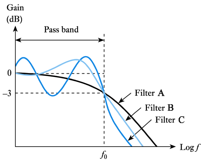
(Continued)
- Common forms include:
- Butterworth
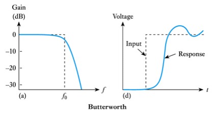
– optimised for a flat response
- Chebyshev
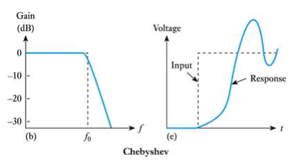
– optimised for a sharp ‘knee’
- Bessel
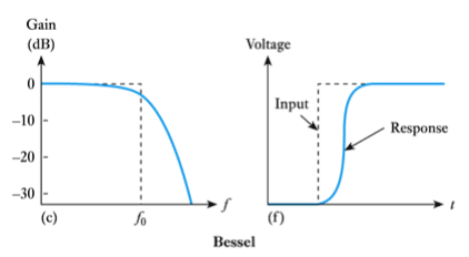
– optimised for its phase response see Section 8.13.3 of the course text for more information on these
Stray Capacitance and Inductance
- All circuits have stray capacitance and stray inductance
– these unintended elements can dramatically affect circuit operation
Filters
- $RC$ Filters
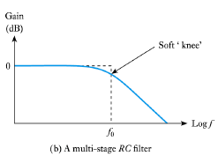
- The $RC$ networks considered earlier are first-order or single-pole filters
– these have a maximum roll-off of 6 dB/octave
– they also produce a maximum of 90° phase shift
- Combining multiple stages can produce filters with a greater ultimate roll-off rates (12 dB, 18 dB, etc.) but such filters have a very soft ‘knee’
- An ideal filter would have constant gain and zero phase shift for frequencies within its pass band , and zero gain for frequencies outside this range (its stop band )
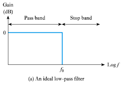
- Real filters do not have these idealised characteristics
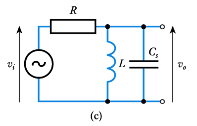
- $LC$ Filters
- Simple $LC$ filters can be produced using series or parallel tuned circuits
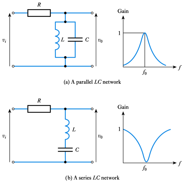
– these produce narrow- band filters with a centre frequency $f_o$
- Active filters
– combining an op-amp with suitable resistors and capacitors can produce a range of filter characteristics
– these are termed active filters
Further Study
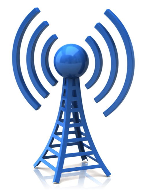
- 🎥 Watch a video on the design of a radio frequency filter - Adobe Flash video
- The Further Study section at the end of Chapter 8 looks at the filter needed to select a single radio station from the multitude being transmitted.
- You are required to design a simple $RLC$ filter to select a given station.
- When you have finished your design watch the video to see why this is not as simple as it perhaps appears.
Key Points
- The reactance of capacitors and inductors is dependent on frequency
- Single $RC$ or $RL$ networks can produce an arrangement with a single upper or lower cut-off frequency
- In each case the angular cut-off frequency $\omega _o$ is given by the reciprocal of the time constant $\text{Τ}$
- For an $RC$ circuit $\text{Τ} = CR$, for an $RL$ circuit $\text{Τ} = L/R$
- Resonance occurs when the reactance of the capacitive element cancels that of the inductive element
- Simple $RC$ or $RL$ networks represent single-pole filters
- Active filters produce high performance without inductors
- Stray capacitance and inductance are found in all circuits
-
- 8.14 Determine the frequencies that correspond to:
(a) an octave below $30$ Hz;
(b) two octaves above $25$ kHz;(c) three octaves above $1$ kHz;(d) a decade above $1$ MHz;(e) two decades below $300$ Hz;(f ) three decades above $50$ Hz.
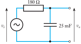
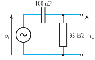
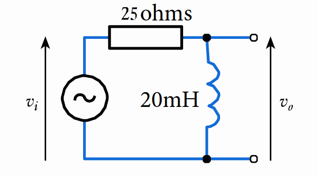
- 8.15 Calculate the time constant $\text{T}$ , the angular cut-off frequency $ \omega _c$ and the cyclic cut-off frequency $ f _c$ of the following arrangement. Is this a high- or a low- frequency cut-off ?
- 8.16 A parallel $RL$ circuit is formed from a resistor of $150 \; \omega$ and an inductor of $30$ mH. What is the time constant of this circuit?
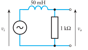
- 8.17 Calculate the time constant $\text{T}$ , the angular cut-off frequency $ \omega _c$ and the cyclic cut-off frequency $ f _c$ of the following arrangement. Is this a high- or a low- frequency cut-off ?
- ⬇Download chapter 8 tutorial
Exercises
- 8.1 What is meant by a ‘two‐port network’, and what are the two ports?
- 8.2 Derive expressions for the voltage gain, current gain and power gain of a two‐port network in terms of the input and output voltages, and the input and output currents.
- 8.3 Determine the voltage gain, current gain and power gain of the following arrangement.
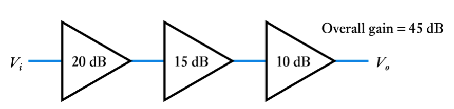
- 8.4 Calculate the overall power gain of the following arrangement if the power gain of each stage is as shown in the diagram.
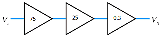
- 8.5 For the arrangement shown in Exercise 8.4, determine the gain of each stage in decibels, and then compute the gain of the overall arrangement in decibels.
- 8.6 A circuit has a gain of $25$ dB. What is its power gain (expressed as a simple ratio)?
- 8.7 A circuit has a gain of $25$ dB. What is its voltage gain?
- 8.8 Calculate the reactance of a $1 \mu F$ capacitor at a frequency of $10$ kHz, and the reactance of a 20 mH inductor at a frequency of $100$ rad/s. In each case include the units in your answer.
- 8.9 Express an angular frequency of $250$ rad/s as a cyclic frequency (in Hz).
- 8.10 Express a cyclic frequency of $250$ Hz as an angular frequency (in rad/s).
- 8.11 Determine the transfer function of the following circuit.
- 8.12 A series $RC$ circuit is formed from a resistor of $33 \; k \; \omega$ and a capacitor or $15 \; nF$. What is the time constant of this circuit?
- 8.13 Calculate the time constant $\text{T}$ , the angular cut-off frequency $\omega _c$ and the cyclic cut-off frequency $f _c$ of the following arrangement. Is this a high- or a low- frequency cut-off ?
- 8.14 Determine the frequencies that correspond to:
-
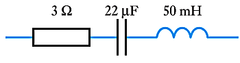
- 8.24 Calculate the resonant frequency $ f _o$, the quality factor $Q$ and the bandwidth B of a parallel circuit with a resistor of $1 \;k \Omega$, an inductor of 50 mH and a capacitor of $22 \; \mu F$.
- 8.25 Why is it more common to construct first order filters using combinations of resistors and capacitors, rather than resistors and inductors.
- 8.26 Explain the difference between a passive and an active filter.
- 8.27 Why are inductors often avoided in the construction of filters?
- 8.28What form of active filter is optimised to produce a flat response within its pass band?
- 8.29 What form of active filter is optimised to produce a sharp transition from the pass band to the stop band?
- 8.30 What form of filter is optimised for a linear phase response?
- 8.31 Explain why stray capacitance and stray inductance affect the frequency response of electronic circuits.
- ⬇ Tutorial Solutions
Exercises (cont.)
- 8.18 Calculate the time constant T , the angular cut-off frequency $ \omega _c$ and the cyclic cut-off frequency $ f _c$ of the following arrangement. Is this a high- or a low- frequency cut-off ?
- 8.19 Sketch a straight-line approximation to the Bode diagram of the circuit of Exercise 8.14. Use this approximation to produce a more realistic plot of the gain and phase responses of the circuit.
- 8.20 A circuit contains three high-frequency cut-offs and two low-frequency cut-offs. What are the rates of change of gain of this circuit at very high and very low frequencies?
- 8.21In the arrangement described in Exercise 8.20, what phase shift is produced at very high and very low frequencies?
- 8.22 Explain what is meant by the term ‘resonance’.
- 8.23 Calculate the resonant frequency $ f _o$ , the quality factor $Q$ and the bandwidth $B$ of the following circuit.